Super-junction power device and manufacturing method thereof

A technology of power devices and conductive types, which is applied in the field of power semiconductor devices, can solve the problems of limited total width of conductive channels, reduce the specific on-resistance of super-junction LDMOS, and achieve low forward conduction resistance, increase width, and reduce resistance. Effect

Inactive Publication Date: 2014-01-15
UNIV OF ELECTRONICS SCI & TECH OF CHINA +1
View PDF4 Cites 8 Cited by
  • Summary
  • Abstract
  • Description
  • Claims
  • Application Information

AI Technical Summary

Problems solved by technology

However, the conductive region of LDMOS is located on the surface of the device. Due to the limitation of surface area, the total width of its conductive channel is limited, which becomes a constraint to further reduce the specific on-resistance of super-junction LDMOS.

Method used


Image

  • Super-junction power device and manufacturing method thereof
  • Super-junction power device and manufacturing method thereof
  • Super-junction power device and manufacturing method thereof

Examples


Embodiment 1

[0038] As a preferred embodiment of the present invention, the present invention discloses a method for preparing a lateral super-junction power device with extremely low specific on-resistance, which includes the following steps:

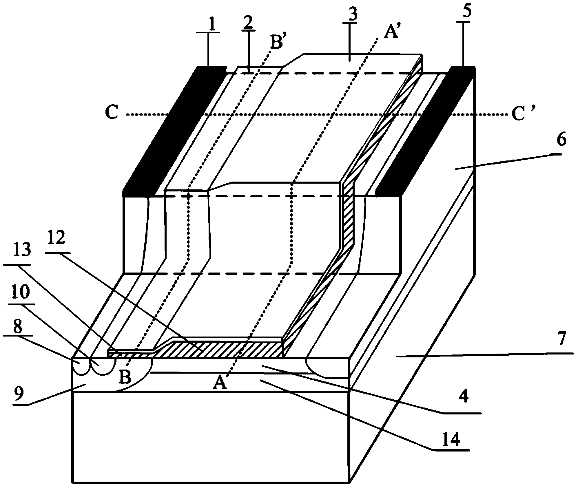
[0039] (1) Preparation of single crystal silicon, using P-type heavily doped region substrate 1, the doping atoms are arsenic, the concentration is 1.5×10 19 cm -3 , whose crystal orientation is ;

[0040] (2) Epitaxial N- epitaxial layer on P+ substrate, such as Figure 5 As shown in , as the substrate auxiliary depletion layer, the dopant atom is phosphorus, and the epitaxial thickness is adjusted according to the requirements of the device electrical parameters;

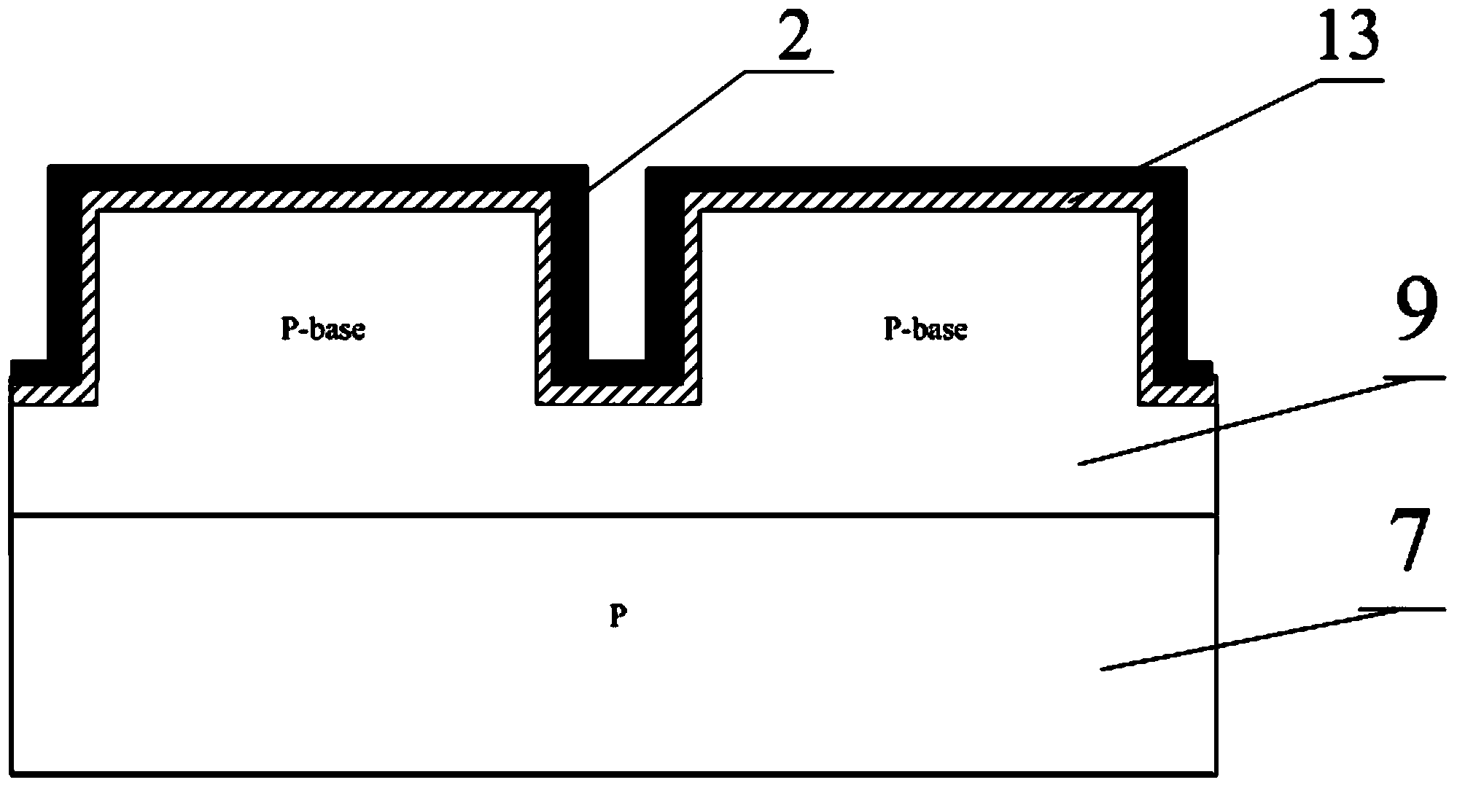
[0041] (3) On the low-resistance N-epitaxial layer, the P-body region and the P-type region are fabricated using boron ion implantation and diffusion processes, such as Figure 6 shown;

[0042] (4) Photolithography, and then use bulk silicon etching to form trench structures in th...

Embodiment 2

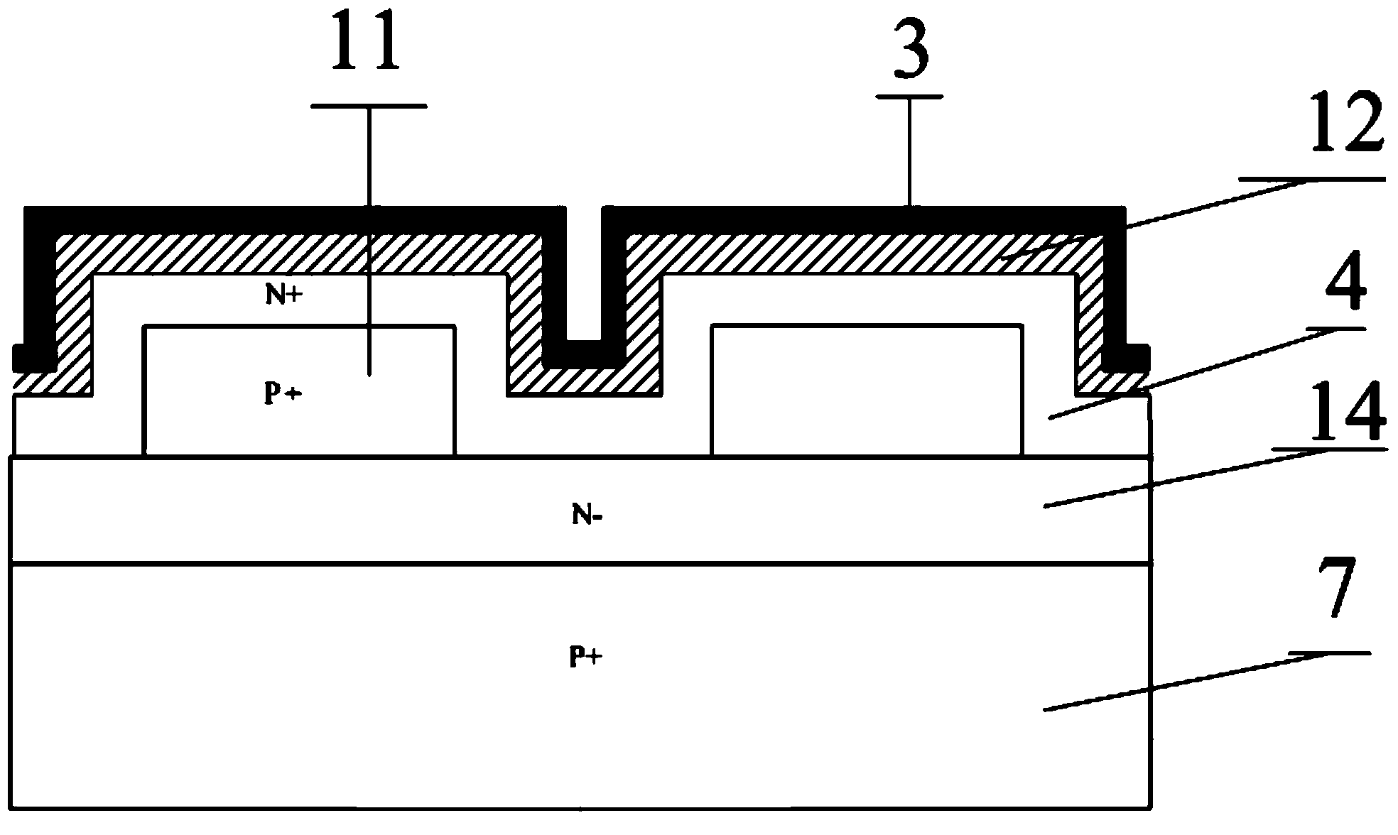
[0050] In this example, on the basis of Example 1, the first conductivity type region 11 can also be Figure 5 In the situation shown, part of the region 11 of the first conductivity type remains between the second conductivity type semiconductor auxiliary depletion layer 14 and the second conductivity type semiconductor region 4 at the groove.

[0051] The specific implementation method of embodiment 2 is similar to embodiment 1, except that in the fifth step of the process steps of embodiment 1, the etching depth of the first conductivity type region 11 is reduced, and the first conductive type region 11 of an appropriate thickness is reserved in the trench groove. Conductivity type region 11.


PUM


Abstract

The invention relates to technologies of power semiconductor devices, in particular to a transverse power device of a super junction structure and a manufacturing method of the transverse power device. The super-junction power device is characterized in that a second conductive type semiconductor drift region 4 and a first conductive type semiconductor body region 9 are provided with grooves, a thick oxidation layer 12 is arranged on the upper surface of the second conductive type semiconductor drift region 4 in a covering mode, a thin gate oxidation layer 13 is arranged on the upper surface of the first conductive type semiconductor body region 9 in a covering mode, and a gate electrode 2 is arranged on the upper surface of the thick oxidation layer 12 and the upper surface of the thin gate oxidation layer 13 in a covering mode. The super-junction power device has the advantages that the area of a channel of an accumulation layer of the surface of the drift region 4 is increased so that lower forward on-resistance can be achieved. The super-junction power device is particularly suitable for transverse power devices of the super junction structure.

Description

technical field [0001] The invention relates to power semiconductor device technology, in particular to a lateral power device with a super junction (Super Junction) structure and a manufacturing method thereof. Background technique [0002] Power semiconductor devices are widely used in DC-DC converters, DC-AC converters, relays, motor drives and other fields. Compared with bipolar transistors, power metal-oxide-semiconductor field effect transistors (MOSFETs) have the advantages of fast switching speed, low loss, high input impedance, and low driving power, especially power MOSFETs have negative The temperature coefficient has no secondary breakdown problem of bipolar transistors, and the safe working area is large, so the application range is wider. [0003] However, conventional power MOSFETs also have their inherent disadvantages, that is, the on-resistance increases with the withstand voltage (R on ∝BV 2.5 ) results in a drastic increase in power dissipation. The e...

Claims


Application Information

Patent Timeline
Patent Type & Authority Applications(China)
IPC IPC(8): H01L29/78H01L29/423H01L21/336
CPCH01L29/0634H01L29/42356H01L29/66681H01L29/7816H01L29/7835H01L29/7834H01L29/42368
Inventor 任敏李果宋询奕顾鸿鸣吴明进张鹏曾智李泽宏张金平张波
Owner UNIV OF ELECTRONICS SCI & TECH OF CHINA
Why Eureka
Try Eureka