Silicon wafer cutting technology

A silicon wafer cutting and crafting technology, applied in the direction of work accessories, manufacturing tools, stone processing equipment, etc., can solve the problem that the mortar cannot meet the cutting process requirements, and achieve the effects of reducing cutting costs, significant economic benefits, and reducing environmental pollution

Active Publication Date: 2014-01-22
SHANXI LUAN PHOTOVOLTAICS TECH
View PDF6 Cites 16 Cited by
  • Summary
  • Abstract
  • Description
  • Claims
  • Application Information

AI Technical Summary

Problems solved by technology

However, during the grinding process, a small part of the edges and corners of the sand grains are damaged and become fine powder, while a large amount of silicon powder, binder powder, glass powder, et

Method used


Image

  • Silicon wafer cutting technology
  • Silicon wafer cutting technology
  • Silicon wafer cutting technology

Examples


Embodiment 1

[0057] 1. Recycling of silicon carbide and cutting fluid

[0058] Through solid-liquid separation, silicon carbide and cutting fluid are recovered, and the standards for recycling silicon carbide and cutting fluid are as follows:

[0059] Standards for the use of recycled silicon carbide:
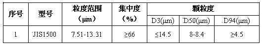
[0060] Graininess:

[0061]

[0062] Among them, D3 means that the proportion of silicon carbide particles with a diameter greater than 14.5 μm is 3%, D50 means that the average particle size of silicon carbide particles is between 8-8.4 μm, and D94 means that 94% of silicon carbide particles have a diameter greater than 4.5 μm.

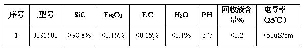
[0063] Requirements for recycling silicon carbide components:

[0064]

[0065] The performance of recycled cutting fluid is as follows:

[0066] Appearance (25°C): Colorless, odorless, transparent liquid;

[0067] chroma: 35;

[0068] Refractive index (20°C): 1.4600;

[0069] ph value (5% aqueous solution): 6.5;

[0070] Moisture ≤0.40%, measured b...

Embodiment 2

[0099] 1. Recycling of silicon carbide and cutting fluid

[0100] Through solid-liquid separation, silicon carbide and cutting fluid are recovered, and the standards for recycling silicon carbide and cutting fluid are as follows:

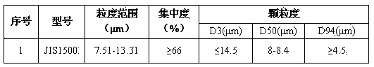
[0101] Standards for the use of recycled silicon carbide:

[0102] Graininess:

[0103]

[0104] Silicon carbide composition requirements:

[0105]

[0106] The performance of recycled cutting fluid is as follows:

[0107] Appearance (25°C): Colorless, odorless, transparent liquid;

[0108] chroma: 30;

[0109] Refractive index (20°C): 1.4620;

[0110] ph value (5% aqueous solution): 6.8;

[0111] Moisture %≤0.40, measured by moisture detector;

[0112] Rotational viscosity (25°C): 43.0mPa?s;

[0113] Density (20°C): 1.115g / cm3, measured by density meter;

[0114] Conductivity (25°C): 6.5 μS / cm.

[0115] 2. Mortar ratio

[0116] Preparation of cutting auxiliary material mortar: the mortar is composed of silicon carbide and cuttin...


PUM

PropertyMeasurementUnit
Densityaaaaaaaaaa
Conductivityaaaaaaaaaa
Diameteraaaaaaaaaa

Abstract

The invention relates to a silicon wafer cutting technology, in particular to a monocrystal silicon and polycrystalline wafer cutting technology suitable for the solar photovoltaic industry. In the silicon wafer cutting technology, main auxiliary materials used for silicon wafer cutting are mortar, waste mortar is recycled, the matching of the mortar is adjusted, and parameters in the cutting technology are adjusted on the basis. The silicon wafer cutting technology has the advantages that the motor is separated and recycled, the use ratio of recycled sand and the use ratio of recycled liquid are improved in the production process, waste materials are recycled, environmental pollution can be reduced, the production cost can be reduced, the photovoltaic industry is accordingly promoted, the solar energy resources are effectively used, and the use number of the non-renewable resources is reduced; the cutting technology is adjusted, the defect that the cutting capacity of the recycled sand and the cutting capacity of the recycled liquid are insufficient is overcome, the silicon wafer cutting pass percent is higher than 92%, the production cost is reduced, and meanwhile discharging of solid waste is reduced.

Description

technical field [0001] The invention relates to a silicon wafer cutting process, which belongs to the technical field of silicon wafer cutting in the solar photovoltaic industry. Background technique [0002] With the development of the photovoltaic industry, the multi-wire cutting process is generally used in the production process of silicon wafers. It uses high-speed moving thin steel wires to carry mortar to grind and cut silicon blocks. The main components of the mortar are cutting fluid and Abrasive composition, the main components of the cutting fluid are polyethylene glycol and other additives; the abrasive is mainly silicon carbide with high hardness. The general ratio of mortar is cutting fluid plus green silicon carbide sand powder (according to 1:0.90-0.95 weight ratio). After the mortar is cut once or more times, the silicon powder generated during the cutting process enters into the mortar and other factors, so it cannot be used any longer, and the old mortar ...

Claims


Application Information

Patent Timeline
IPC IPC(8): B28D5/04B28D7/00
Inventor 周水生曹彦民张爱民董建明刘亚军刘进任崇荣李东东刘宝华黄伦杰
Owner SHANXI LUAN PHOTOVOLTAICS TECH
Why Eureka
Try Eureka