Preparation method for island-actuated single-electron transistor

A single-electron transistor and island-driven technology, which is applied in semiconductor/solid-state device manufacturing, circuits, electrical components, etc., to reduce difficulty and achieve the effect of precise assembly

Inactive Publication Date: 2014-01-22
NAT UNIV OF DEFENSE TECH
View PDF3 Cites 6 Cited by
  • Summary
  • Abstract
  • Description
  • Claims
  • Application Information

AI Technical Summary

Problems solved by technology

[0005] However, there are three key technical problems in the current preparation of single-electron transistors: the controllable preparation of small-sized Coulomb islands; the controllable positioning and assembly of Coulomb islands; the precise control of the size of the tunneling barrier between Coulomb islands and electrodes.

Method used


Image

  • Preparation method for island-actuated single-electron transistor
  • Preparation method for island-actuated single-electron transistor
  • Preparation method for island-actuated single-electron transistor

Examples


Embodiment 1

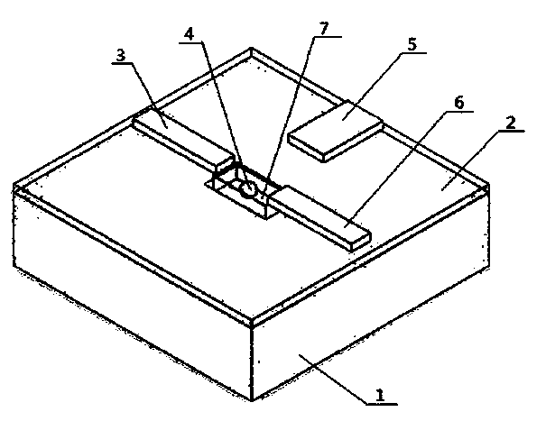
[0030] Island-driven single-electron transistor fabrication:

[0031] (1) cleaning the silicon substrate 1;

[0032] (2) Oxidize the silicon substrate 1 for 2 hours at 1000°C in an oxidation furnace to form a silicon dioxide insulating layer on the surface of the silicon substrate 1 as the substrate 2, and the thickness of the silicon dioxide insulating layer is about 200 nm;

[0033] (3) The source 3, the drain 6 and the gate 5 were prepared on the substrate 2 by electron beam exposure and evaporation coating method. At this time, Ti was used as the metal adhesion layer, and the thickness of the adhesion layer was about 2 nm. Au is used as the deposition material, and the thickness of the deposition material is about 5 nm, wherein the minimum line width of the electrode is about 25 nm, and the distance between the source and the drain on the substrate is about 30 nm; The spacing on the substrate is about 50 nm; and on the substrate 2, the island-moving single Electronic tra...

Embodiment 2

[0045] Island-driven single-electron transistor fabrication:

[0046] (1) cleaning the silicon substrate 1;

[0047] (2) Oxidize the silicon substrate 1 in an oxidation furnace at 1000°C for 2 hours, so that a silicon dioxide insulating layer as the substrate 2 is formed on the surface of the silicon substrate 1, and the thickness of the silicon dioxide insulating layer is about 300 nm;

[0048] (3) The source 3, drain 6 and gate 5 are prepared on the substrate 2 by focused ion beam / electron beam induced deposition. At this time, Pt or W is used as the deposition material, and the thickness of the deposition material is 15-30 nm , wherein the minimum line width of the electrode is about 25 nm, the distance between the source and drain on the substrate is about 30 nm; the distance between the gate and the source and drain on the substrate is about 300 nm; and by Ordinary photolithography or focused ion beam deposition prepares on the substrate 2 micron-scale leads connected to...

Embodiment 3

[0060] Island-driven single-electron transistor fabrication:

[0061] (1) cleaning the silicon substrate 1;

[0062] (2) Oxidize the silicon substrate 1 for 2 hours at 1000°C in an oxidation furnace to form a silicon dioxide insulating layer on the surface of the silicon substrate 1 as the substrate 2, and the thickness of the silicon dioxide insulating layer is about 500 nm;

[0063] (3) The source 3, the drain 6 and the gate 5 were prepared on the substrate 2 by electron beam exposure and evaporation coating method. At this time, Ti was used as the metal adhesion layer, and the thickness of the adhesion layer was about 3 nm. Au is the deposition material, and the thickness of the deposition material is about 25 nm, wherein the minimum line width of the electrode is about 25 nm, and the distance between the source and the drain on the substrate is about 30 nm; The spacing on the substrate is about 500 nm; and the island-moving single Electronic transistor devices transition...


PUM


Abstract

The invention discloses a preparation method for an island-actuated single-electron transistor. The method takes a silicon chip, a source, a drain, a gate, an island area and a coulomb island as the basic structure of a single-electron transistor. The source, the drain and the gate are integrally arranged on the silica substrate formed at the surface of the silicon chip; the island area is etched in the area enclosed by the source, the drain and the gate; and the coulomb island is installed in the island and can move in the island. The island area is prepared by means of focusing ion beam etching or reactive ion etching; the coulomb island can move in the island area under the effects of an electric field; the tunneling potential barrier between electrodes and the coulomb island changes with the electric field; and the coulomb island is prepared through a colloid Au preparation process so that the dimension is controllable. The device finally exhibits comprehensive effects of field emission and coulomb obstruction. By using the method, the size and the assembling positioning of the coulomb island can be accurately controlled, the problem of accurate control needed by a potential barrier layer can be avoided, and the preparation difficulty of the single-electron transistor is remarkably reduced.

Description

technical field [0001] The invention relates to the technical field of nanometer electronic devices, in particular to a method for preparing an island-type single-electron transistor. Background technique [0002] The characteristic size of the integrated circuit with metal oxide semiconductor field effect transistor devices as the mainstream has been developed to the nanometer level, and the application is limited. Further research and development of new nanometer-sized electronic logic devices has become a development demand. Among the current main nano single-electron devices, single-electron transistors have attracted much attention due to their advantages of small size, high sensitivity and low power consumption. It can realize logic operations and information storage at the nanoscale, and is a new nanoelectronic device based on the Coulomb blocking effect and single-electron tunneling effect. [0003] The study of single-electron phenomenon was carried out earlier in...

Claims


Application Information

Patent Timeline
Patent Type & Authority Applications(China)
IPC IPC(8): H01L21/334B82Y10/00
CPCB82Y10/00H01L29/66439
Inventor 方靖岳秦石乔张学骜秦华王飞王广陈卫罗威邵铮铮贾红辉常胜利
Owner NAT UNIV OF DEFENSE TECH
Why Eureka
Try Eureka