LED epitaxy structure and preparation method thereof

An epitaxial structure, N-type technology, applied in the direction of electrical components, circuits, semiconductor devices, etc., can solve the problems of GaN-based epitaxial structure process complexity, high manufacturing cost, etc., to increase carrier concentration and mobility, and reduce interface free energy , Improve the effect of crystal quality

Active Publication Date: 2014-01-22
SUZHOU JUZHEN PHOTOELECTRIC
View PDF6 Cites 23 Cited by
  • Summary
  • Abstract
  • Description
  • Claims
  • Application Information

AI Technical Summary

Problems solved by technology

[0005] Therefore, what the present invention aims to solve is the problem of complex process and high preparation cost of GaN-based epitaxial structure in the p...

Method used


Image

  • LED epitaxy structure and preparation method thereof
  • LED epitaxy structure and preparation method thereof
  • LED epitaxy structure and preparation method thereof

Examples


Embodiment

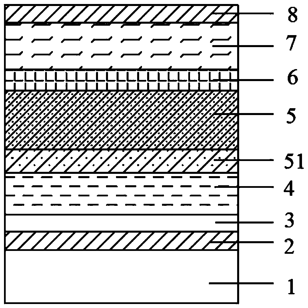
[0046] This invention may be embodied in many different forms and should not be construed as limited to the embodiments set forth herein. Rather, these embodiments are provided so that this disclosure will be thorough and complete and will fully convey the concept of the invention to those skilled in the art, and the present invention will only be defined by the appended claims. In the drawings, the size and relative sizes of layers and regions may be exaggerated for clarity. It will be understood that when an element such as a layer is referred to as being "formed on" or "disposed on" another element, it can be directly on the other element or intervening elements may also be present. In contrast, when an element is referred to as being "directly formed on" or "directly disposed on" another element, there are no intervening elements present.

[0047] The equipment adopted in the metal organic chemical vapor deposition process described in the following examples and comparati...


PUM

PropertyMeasurementUnit
Thicknessaaaaaaaaaa
Thicknessaaaaaaaaaa
Thicknessaaaaaaaaaa

Abstract

The invention relates to an LED (light-emitting diode) epitaxy structure. An N-type GaN layer adopts a peridoic gradient doped structure; Si doped GaN layers and undoped GaN layers are alternately arranged; electrons can be gathered in the undoped GaN layers to form high-density two-dimensional electron gas, so that the concentration and mobility of a carrier are effectively improved; a more important fact is that a multijunction capacitance structure is formed between a U-shaped superlattice layer on a multiple quantum well layer and the N-type GaN layer; the transverse expansion ability of the carrier can be effectively improved; the distribution area of current flowing into the multiple quantum well layer is enlarged; and LED driving voltage is effectively reduced. The invention further relates to a preparation method of the LED epitaxy structure. The N-type GaN layer is simple in doped structure and small in layer number; the superlattice layer adopts an undoped structure; a technology is simple; and the manufacturing cost is low.

Description

technical field [0001] The invention relates to the technical field of semiconductors, in particular to an epitaxial structure capable of reducing LED forward voltage drop, improving luminous efficiency and service life and a preparation method thereof. Background technique [0002] Gallium nitride (GaN)-based light-emitting diodes (Light-Emitting Diode, LED) have the advantages of long life, low power consumption, and no pollution, and can be used in many fields such as display and lighting. Although GaN-based LEDs have been industrialized, the problems of high forward voltage drop and low luminous efficiency of LED chips have not been well resolved due to the existing LED epitaxial structure and its preparation method. [0003] Chinese patent CN103187497A discloses an epitaxial structure and its growth method for improving the light efficiency of large-scale chips, specifically: growing a GaN buffer layer on PSS (Patterned Sapphire Substrate, translated as: patterned sapph...

Claims


Application Information

Patent Timeline
IPC IPC(8): H01L33/04H01L33/06H01L33/00
CPCH01L33/0075H01L33/04H01L33/14
Inventor 李勇崔德国
Owner SUZHOU JUZHEN PHOTOELECTRIC
Why Eureka
Try Eureka