

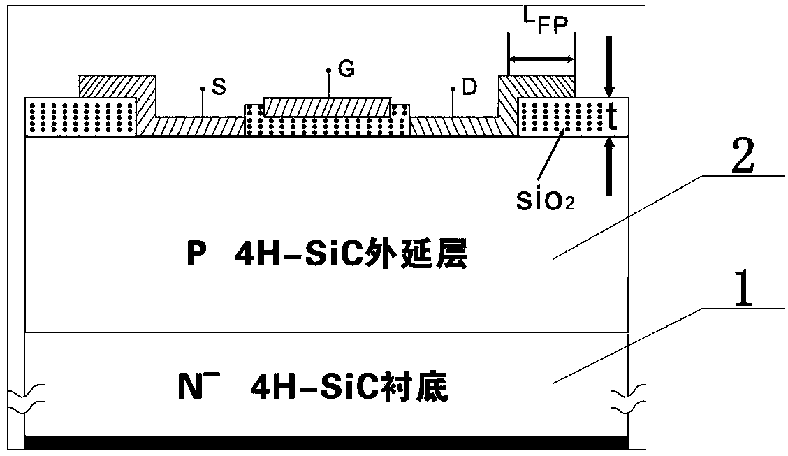
4H-SiC Schottky barrier source/drain MOSFET device with field plate terminal protection and manufacturing method thereof
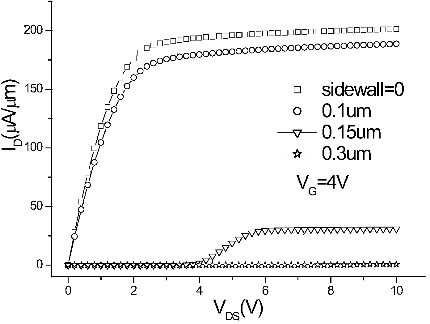
A terminal protection, 4h-sic technology, applied in semiconductor/solid-state device manufacturing, semiconductor devices, electrical components, etc., can solve the problems of low mobility of the inversion layer, deterioration of device on-resistance output characteristics, etc., and achieve saturation current Reduce, reduce transconductance, reduce the effect of source-drain series resistance
- Summary
- Abstract
- Description
- Claims
- Application Information
AI Technical Summary
Problems solved by technology
Method used
Image

Examples
Embodiment Construction
[0028] In order to make the object, technical solution and advantages of the present invention more clear, the present invention will be further described in detail below in conjunction with the examples. It should be understood that the specific embodiments described here are only used to explain the present invention, not to limit the present invention.
[0029] The application principle of the present invention will be further described below in conjunction with the accompanying drawings and specific embodiments.
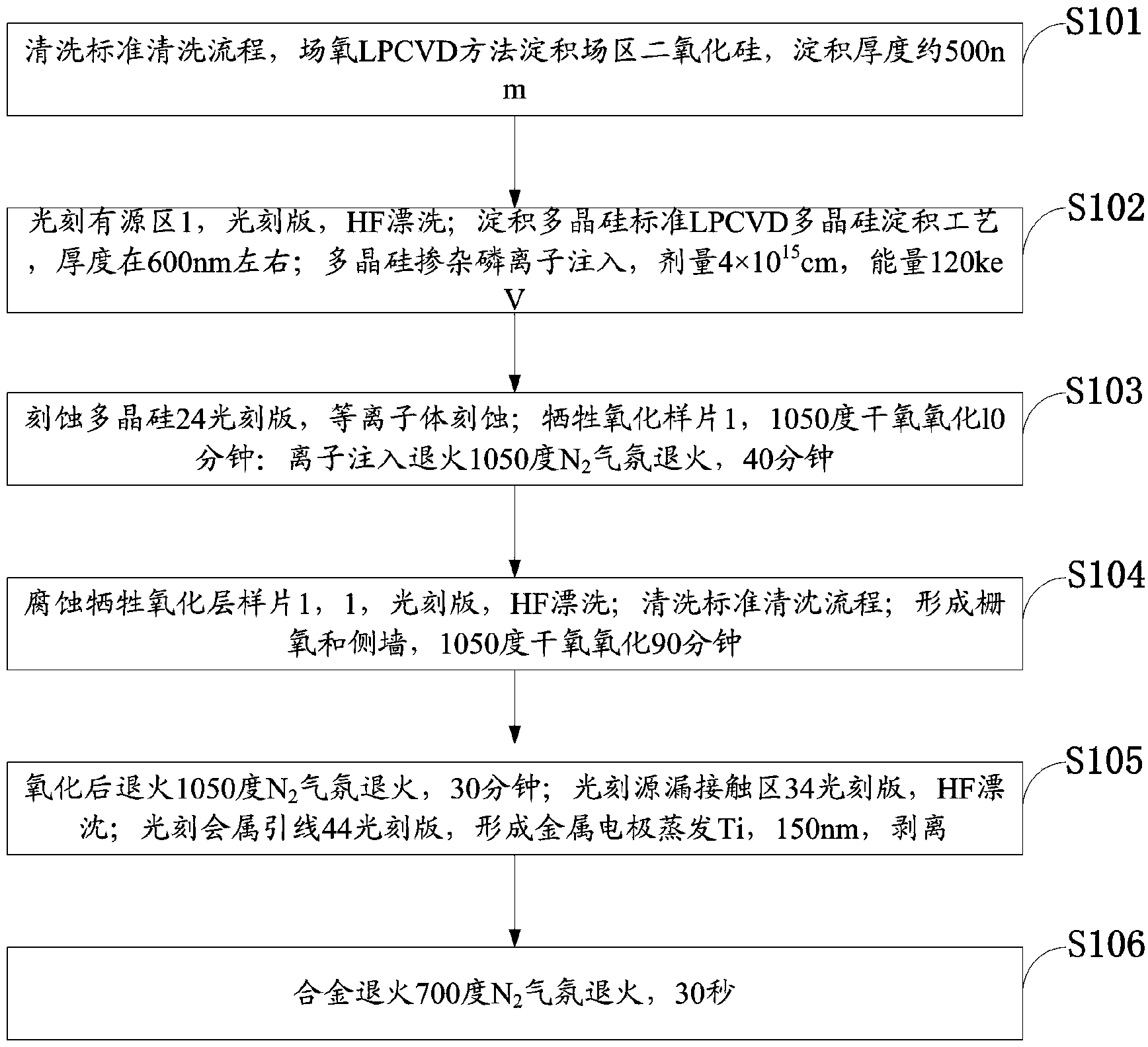
[0030] Such as figure 1 As shown, the preparation method of the 4H-SiC Schottky source-drain MOSFET device with field plate termination protection according to the embodiment of the present invention includes the following steps:
[0031] The preparation method of the 4H-SiC Schottky source-drain MOSFET device with field plate termination protection of the present invention requires four photolithography masks, and the basic description is as follows:
[0032] ...
PUM
 Abstract
Description
Claims
Application Information