Semiconductor device and manufacturing method thereof

A device manufacturing method and semiconductor technology, applied in semiconductor/solid-state device manufacturing, semiconductor devices, transistors, etc., can solve the problems of reduced filling space, insufficient filling of gate resistors, and difficulty in effectively reducing the size of the resistance adjustment layer. Achieve the effect of increasing the filling space, reducing the gate resistance, and simplifying the structure of the PMOS metal gate

Active Publication Date: 2014-02-12
INST OF MICROELECTRONICS CHINESE ACAD OF SCI
View PDF5 Cites 11 Cited by
  • Summary
  • Abstract
  • Description
  • Claims
  • Application Information

AI Technical Summary

Problems solved by technology

In this way, in the device structure of the PMOS region, the metal gate structure is extremely complex (containing three barrier layers), and under the condition that the feature size-gate length is gradually reduced, especially when the gate length is below 22nm, at this time due to many The structure of the layer barrier layer reduces the space that can be filled by the resistance adjustment layer in the PMOS region, and there are problems that the resistance adjustment layer is small and difficult to effectively reduce the gate resistance, and insufficient filling causes holes to increase the resistivity.

Method used


Image

  • Semiconductor device and manufacturing method thereof
  • Semiconductor device and manufacturing method thereof
  • Semiconductor device and manufacturing method thereof

Examples


Embodiment Construction

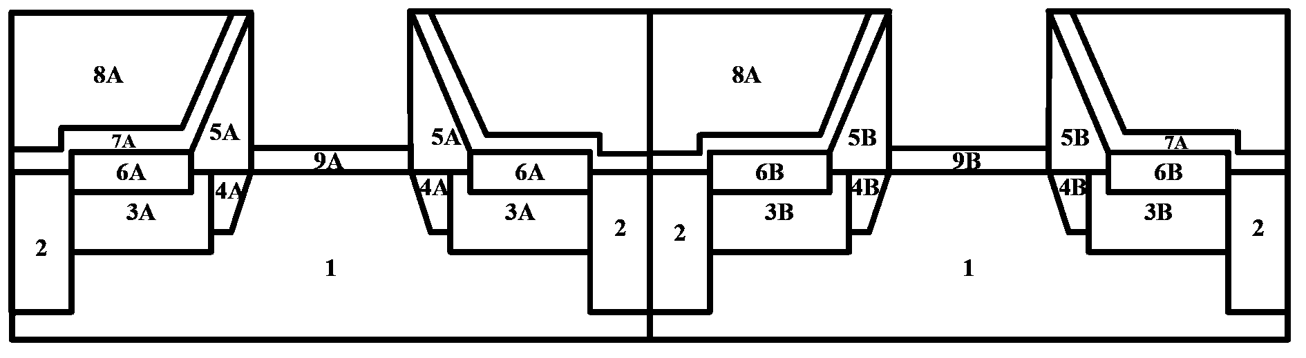
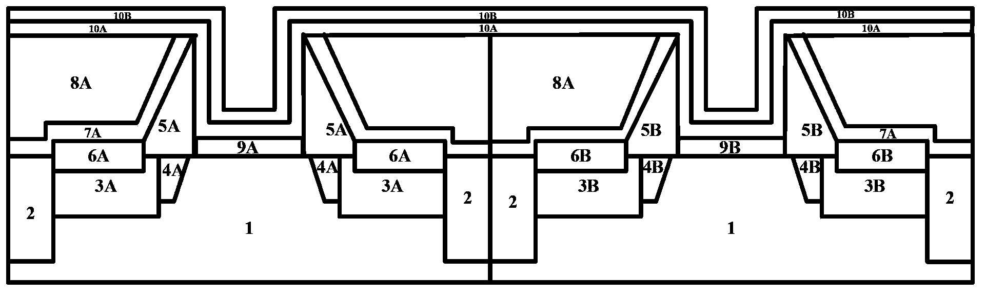
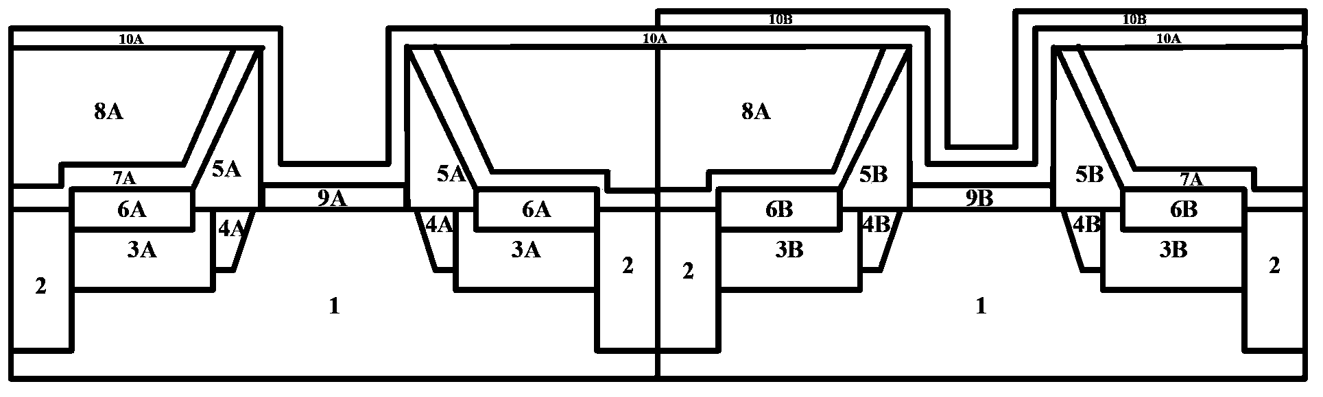
[0025] The features and technical effects of the technical solution of the present invention will be described in detail below with reference to the accompanying drawings and in conjunction with schematic embodiments, disclosing a CMOS that can effectively control the work function of a metal gate while effectively reducing gate resistance and a manufacturing method thereof. It should be pointed out that similar reference numerals represent similar structures, and the terms "first", "second", "upper", "lower" and the like used in this application can be used to modify various device structures or manufacturing processes . These modifications do not imply spatial, sequential or hierarchical relationships of the modified device structures or fabrication processes unless specifically stated.

[0026] The following will refer to Figure 1 to Figure 7 A cross-sectional schematic diagram is used to describe in detail the steps of the CMOS manufacturing method according to the presen...


PUM


Abstract

The invention discloses a semiconductor device which comprises a substrate, a plurality of grid stacking structures, a plurality of grid sidewall structures and a plurality of source-drain regions. The grid stacking structures are arranged on the substrate. The two sides of each grid stacking structure are provided with the grid sidewall structures. The positions, on the two sides of each grid sidewall structure, of the substrate are provided with the source-drain regions. The grid stacking structures comprise a plurality of first grid stacking structures and a plurality of second grid stacking structures. The semiconductor device is characterized in that each first grid stacking structure comprises a first grid insulation layer, a first blocking layer, a first work function regulating layer and a resistance regulating layer, and each second grid stacking structure comprises a second grid insulation layer, the first blocking layer, a second work function regulating layer, the first work function regulating layer and the resistance regulating layer. According to the semiconductor device and a manufacturing method thereof, firstly, an NMOS work function regulating layer is selectively deposited, and then a PMOS work function regulating layer is deposited. Consequently, a PMOS metal grid structure is simplified, metal grid work functions are effectively controlled, meanwhile, the filled spaces of the resistance regulating layers are enlarged, and the grid resistance is effectively reduced.

Description

technical field [0001] The invention relates to a semiconductor device and a manufacturing method thereof, in particular to a CMOS with more effective control of work function and reduced gate resistance and a manufacturing method thereof. Background technique [0002] Starting from the 45nm CMOS integrated circuit process, with the continuous reduction of device feature size, in order to suppress the short channel effect, the equivalent oxide thickness (EOT) of the gate insulating dielectric layer in CMOS devices must be reduced simultaneously. However, due to the low (relative) dielectric constant (for example, about 3.9) of the ultra-thin (eg 10nm) conventional oxide layer or oxynitride layer, the insulation performance is difficult to withstand the relatively high field strength in such ultra-small devices, which will cause serious damage. gate leakage. Therefore, the traditional polysilicon (poly-si) / SiON system is no longer applicable. [0003] In view of this, the i...

Claims


Application Information

Patent Timeline
Patent Type & Authority Applications(China)
IPC IPC(8): H01L29/423H01L27/092H01L21/28H01L21/8238
CPCH01L29/66545H01L29/4966H01L21/823842H01L29/42356H01L21/285H01L21/8238H01L27/092
Inventor 殷华湘闫江陈大鹏
Owner INST OF MICROELECTRONICS CHINESE ACAD OF SCI
Why Eureka
Try Eureka