Organic electroluminescent device and preparation method thereof
An electroluminescent device and luminescent technology, which is applied in the direction of electric solid-state devices, semiconductor/solid-state device manufacturing, electrical components, etc., can solve problems such as failure, short life of organic electroluminescent devices, and material aging, and achieve long life, Improve the waterproof oxygen capacity and reduce the effect of damage
- Summary
- Abstract
- Description
- Claims
- Application Information
AI Technical Summary
Problems solved by technology
Method used
Image
Examples
preparation example Construction
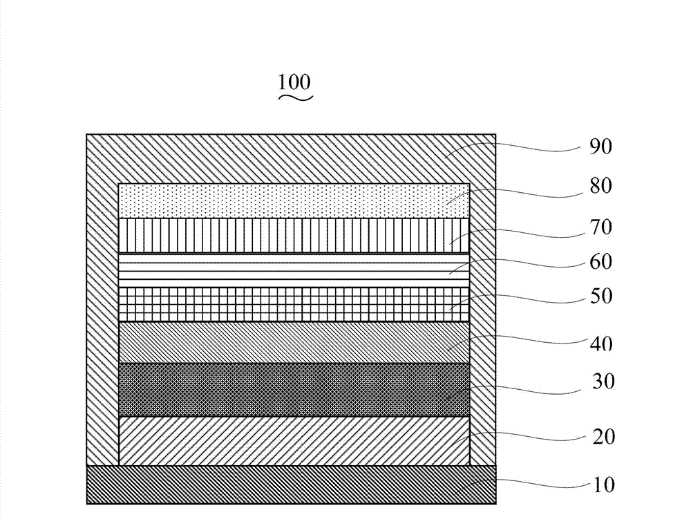
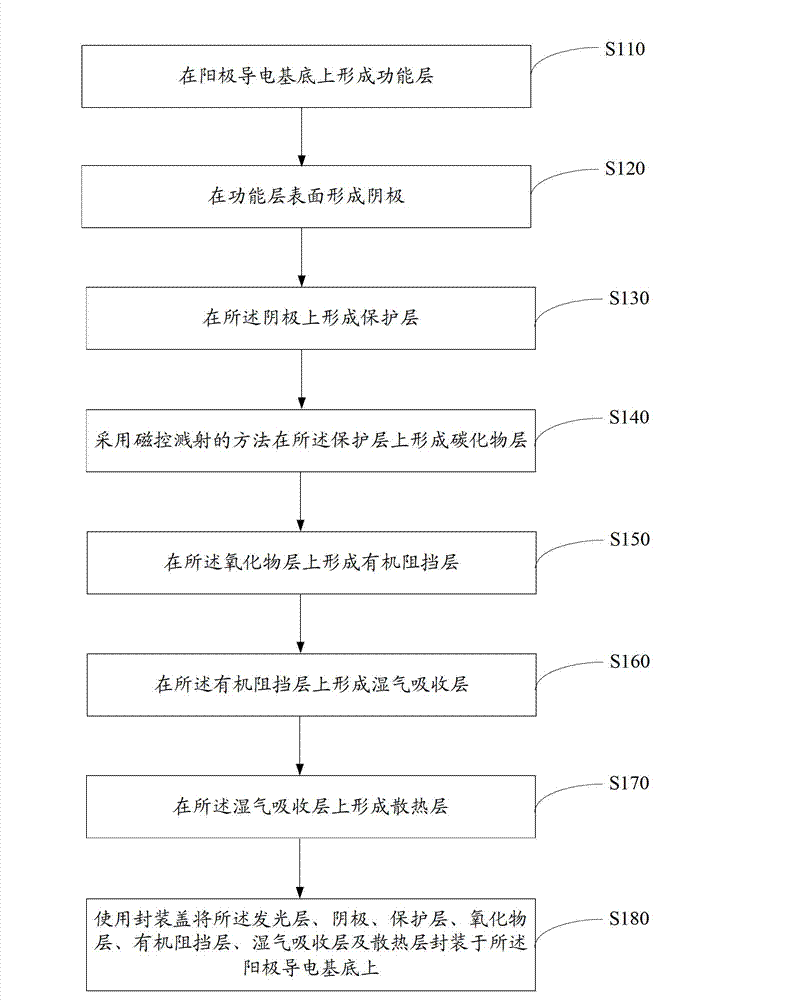
[0050] see figure 2 , the preparation method of the above-mentioned organic electroluminescent device 100 includes the following steps:
[0051] Step S110 , forming a functional layer 20 on the anode conductive substrate 10 .
[0052] The anode conductive substrate 10 may be a glass conductive substrate or a conductive organic polyethylene terephthalate (PET) film substrate. The anode conductive substrate 10 has an ITO layer prepared with an anode pattern. The thickness of the ITO layer is 100nm~150nm.
[0053] The surface of the anode conductive substrate 10 is pretreated before the functional layer 20 is formed to remove the pollutants on the surface of the anode conductive substrate 10, and surface activation is performed to increase the oxygen content on the surface of the anode conductive substrate 10 to improve the work function of the surface of the anode conductive substrate 10 . Specifically, the anode conductive substrate 10 is ultrasonically cleaned with aceton...
Embodiment 1
[0082] The preparation structure is: ITO / NPB: MoO 3 / TCTA / TPBI: Ir(ppy) 3 / Bphen / Bphen:CsN 3 / Al / CuPc / (SiC / PTFE) 3 / CaO / Cu / organic electroluminescent devices with encapsulation caps.
[0083] The preparation method of the above-mentioned organic electroluminescent device comprises the following steps:
[0084] 1. Forming a functional layer on a conductive substrate.
[0085] The conductive substrate 10 is a glass conductive substrate. The conductive substrate 10 has an ITO layer prepared with an anode pattern. The thickness of the ITO layer was 100 nm.
[0086] Before forming the functional layer 20, the surface of the conductive substrate 10 is pretreated to remove pollutants on the surface of the substrate 10, and the surface is activated to increase the oxygen content on the surface of the conductive substrate 10 to improve the work function of the surface of the conductive substrate 10. Specifically, the conductive substrate 10 is ultrasonically cleaned for 5 minut...
Embodiment 2
[0108] The preparation structure is: ITO / NPB: MoO 3 / TCTA / TPBI: Ir(ppy) 3 / Bphen / Bphen:CsN 3 / Al / NPB / (WC / methacrylic resin) 3 / BaO / Ag / organic electroluminescent devices with capsulation.
[0109] 1. Forming a functional layer on a conductive substrate.
[0110] The conductive substrate 10 is a glass conductive substrate. The conductive substrate 10 has an ITO layer prepared with an anode pattern. The thickness of the ITO layer was 100 nm.
[0111] Before forming the functional layer 20, the surface of the conductive substrate 10 is pretreated to remove pollutants on the surface of the substrate 10, and the surface is activated to increase the oxygen content on the surface of the conductive substrate 10 to improve the work function of the surface of the conductive substrate 10. Specifically, the conductive substrate 10 is ultrasonically cleaned for 5 minutes with acetone-free, ethanol, ionized water and ethanol in sequence, and then blown dry with nitrogen and oven-dried...
PUM
| Property | Measurement | Unit |
|---|---|---|
| Thickness | aaaaa | aaaaa |
| Thickness | aaaaa | aaaaa |
| Thickness | aaaaa | aaaaa |
Abstract
Description
Claims
Application Information


