Method for manufacturing superconducting cavity

A technology of superconducting cavity and superconducting material, which is applied in the manufacturing field of radio frequency superconducting accelerating cavity (referred to as superconducting cavity), which can solve the problems of manufacturing failure, high-frequency performance degradation of superconducting cavity, and high welding risk, so as to improve the quality of finished products. High-frequency and high-frequency characteristics, guaranteed purity and high-frequency characteristics, and the effect of simplifying the processing technology

Active Publication Date: 2014-03-05
INST OF MODERN PHYSICS CHINESE ACADEMY OF SCI
View PDF4 Cites 13 Cited by
  • Summary
  • Abstract
  • Description
  • Claims
  • Application Information

AI Technical Summary

Problems solved by technology

[0011] Using the above method to manufacture a superconducting cavity has the following problems: (1) the process is complicated and the cycle is long, and it generally takes one year to manufacture a superconducting cavity with a new structure or new parameters; (2) it is easy to scratch and pollute niobium during the manufacturing process (3) Due to the rebound characteristics of niobium materials, it is difficult to meet the

Method used


Image

  • Method for manufacturing superconducting cavity
  • Method for manufacturing superconducting cavity
  • Method for manufacturing superconducting cavity

Examples


Embodiment 1

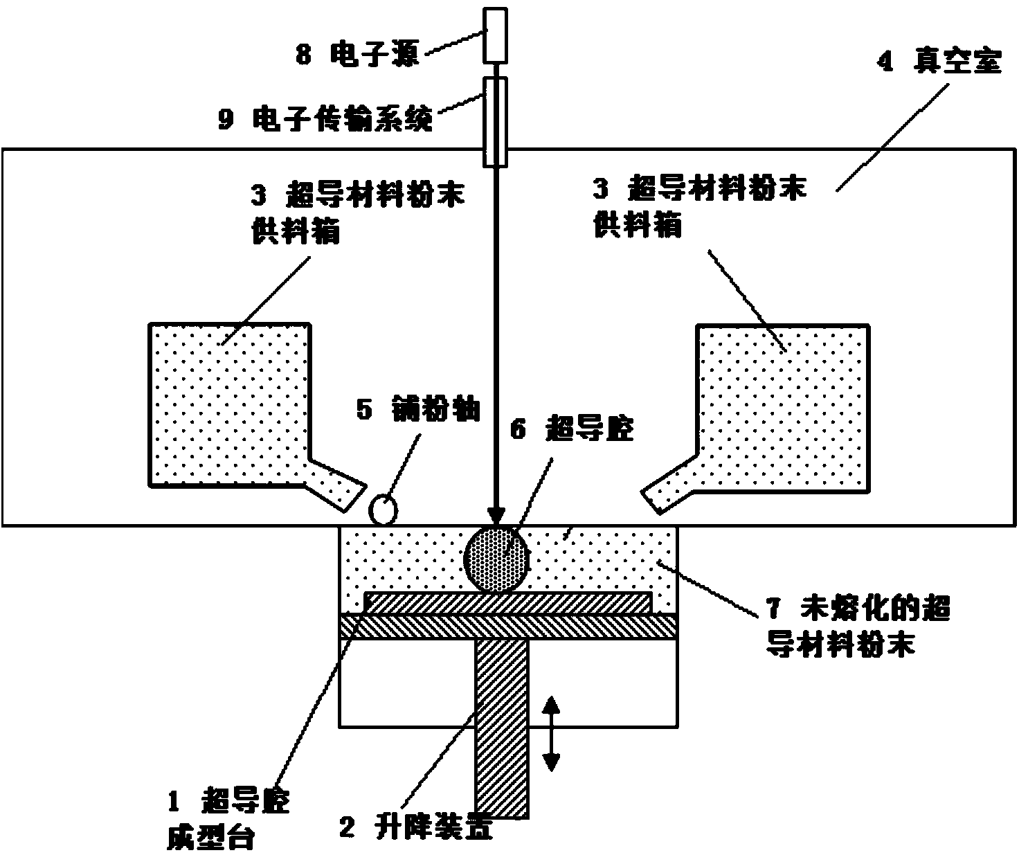
[0035] Example 1: See figure 1 , A method for preparing a high-purity niobium superconducting cavity, which mainly includes the following steps:

[0036] (1) Preparation:

[0037] 1) The raw material is high-purity niobium powder: the high-purity niobium powder is obtained by reducing niobium oxide, the particle size of the powder is 10nm-20μm, and the purity is 99%-99.99%;

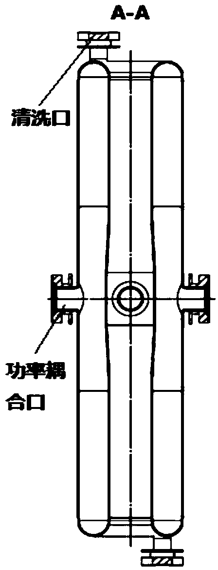
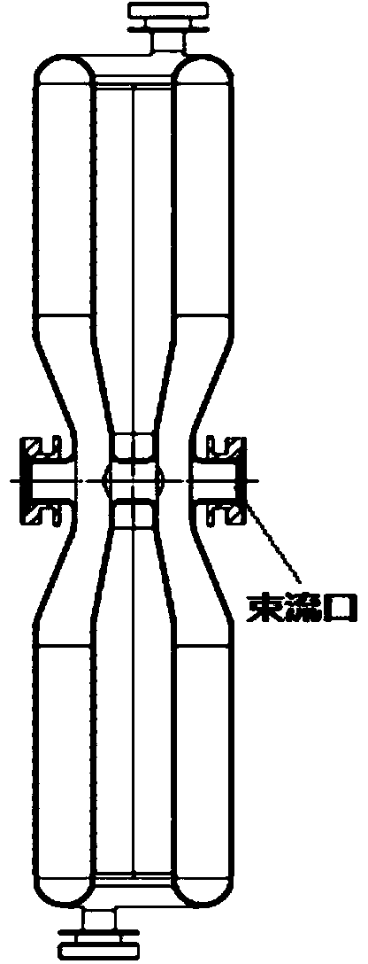
[0038] 2) Use CAD software to generate a superconducting cavity model, taking a half-wavelength cavity as an example, see figure 2 with image 3 , Use layering software to layer them, each slice layer describes the cross section of the superconducting cavity with a certain height of 0.05-0.3mm;

[0039] 3) Use a vacuum system to provide a vacuum environment in the molding device, and the vacuum degree of the vacuum chamber is better than 1×10 -3 Pa;

[0040] 4) Spread the high-purity niobium powder from step 1) on the workbench in the molding room;

[0041] 5) Use the control system to "print" the electron beam en...

Embodiment 2

[0050] Embodiment 2: Nb proposed by the present invention 3 The embodiment of the manufacturing method of Sn superconducting cavity is described in detail as follows:

[0051] 1 Preparation:

[0052] (1) The raw material used is Nb 3 Sn powder, the particle size of the powder is 10nm-20μm, and the purity is 99%-99.99%;

[0053] (2) Use CAD and SolidWorks software to draw the superconducting cavity model, take half-wavelength cavity as an example, see figure 2 with image 3 , Use layering software to layer them, each slice layer has a height of 0.05-0.3mm, and each slice layer describes the cross section of the superconducting cavity with a certain height;

[0054] (3) See the process of manufacturing superconducting cavity by electron beam melting figure 1 , The superconducting material powder supply box 3 provides Nb for the molding room 3 Sn powder, powder spreading shaft 5 will be Nb in the molding room 3 The Sn powder is flattened and controlled by the microcomputer software. The...

Embodiment 3

[0061] Example 3: See figure 1 , A MgB 2 The preparation method of the superconducting cavity mainly includes the following steps:

[0062] (1) Preparation:

[0063] 1) The raw material is MgB 2 Powder: The particle size of the powder is 10nm-20μm, and the purity is 99%-99.99%:

[0064] 2) Use CAD software to generate a superconducting cavity model, taking a half-wavelength cavity as an example, see figure 2 with image 3 , Use layering software to layer them, each slice layer describes the cross section of the superconducting cavity with a certain height of 0.05-0.3mm;

[0065] 3) Use a vacuum system to provide a vacuum environment in the molding device, and the vacuum degree of the vacuum chamber is better than 1×10 -3 Pa;

[0066] 4) Change the MgB of step 1) 2 Spread the powder on the workbench in the forming room;

[0067] 5) Use the control system to "print" the electron beam energy onto the powder layer according to the software model description of the superconducting cavity sl...


PUM

PropertyMeasurementUnit
Granularityaaaaaaaaaa

Abstract

The invention mainly relates to manufacturing of a radio frequency superconducting accelerating cavity. A method for manufacturing a superconducting cavity includes the steps that CAD software is utilized to generate a superconducting cavity model, and layering software is utilized to conduct layering on the superconducting cavity model; a vacuum system is utilized to provide a vacuum environment for a forming chamber; a forming table of the forming chamber is paved with superconducting material powder; according to description of a software model of a superconducting cavity slice layer, electron beam energy is 'printed' on a powder layer, and a superconducting material slice layer entity is generated and becomes a part of the superconducting cavity; a next slice layer continues to be machined on the first slice layer entity until the whole machining process of the superconducting cavity is finished. According to the method, the development cycle of the superconducting cavity is shortened; no welding joint exists in the whole superconducting cavity, and the development yield of the superconducting cavity is increased; purity of superconducting materials can be guaranteed; the superconducting cavity is not limited by stamping forming conditions, and the performance of the superconducting cavity can be improved; in the manufacturing process, the redundant superconducting material powder can be reutilized, and therefore production cost is lowered.

Description

Technical field [0001] The invention belongs to the technical field of particle accelerators, and particularly relates to a method for manufacturing a radio frequency superconducting acceleration cavity (superconducting cavity for short). Background technique [0002] Compared with the room temperature acceleration cavity, the superconducting acceleration cavity has the advantages of high acceleration efficiency and low high-frequency heat loss. The superconducting accelerator cavity has become the core component of large scientific devices such as linear colliders, free electron lasers, spallation neutron sources, advanced light sources, and accelerator-driven nuclear energy transmutation devices (ADS). The world has developed a variety of superconducting cavity types such as ellipsoid cavity, Spoke cavity, half-wavelength cavity (HWR), quarter-wavelength cavity (QWR), etc. At present, the raw materials used in the production of basically all types of superconducting cavities ar...

Claims


Application Information

Patent Timeline
IPC IPC(8): H05H7/00B22F3/105C04B35/58
Inventor 何源张生虎岳伟明
Owner INST OF MODERN PHYSICS CHINESE ACADEMY OF SCI
Why Eureka
Try Eureka