Method for improving silicon chip warping degree

A warpage, silicon wafer technology, used in electrical components, semiconductor/solid-state device manufacturing, circuits, etc., to solve problems such as debris and constant silicon wafer alarms

Active Publication Date: 2014-03-12
SHANGHAI HUAHONG GRACE SEMICON MFG CORP
View PDF3 Cites 5 Cited by
  • Summary
  • Abstract
  • Description
  • Claims
  • Application Information

AI Technical Summary

Problems solved by technology

It will not only cause silicon wafers to continue to alarm in the subsequent process, but also seriously risk fragmentation

Method used


Image

  • Method for improving silicon chip warping degree
  • Method for improving silicon chip warping degree
  • Method for improving silicon chip warping degree

Examples


Embodiment Construction

[0023] see Figure 7 As shown, in the following embodiments, the method for improving the warpage of silicon wafers includes the following steps:

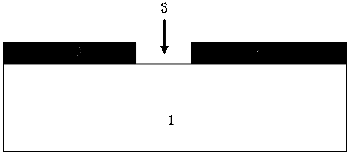
[0024] Step 1. Combine figure 1 As shown, a pre-metal dielectric layer 2 is formed on a silicon substrate 1 , and a contact hole 3 penetrating through the pre-metal dielectric layer 2 is formed in the pre-metal dielectric layer 2 .

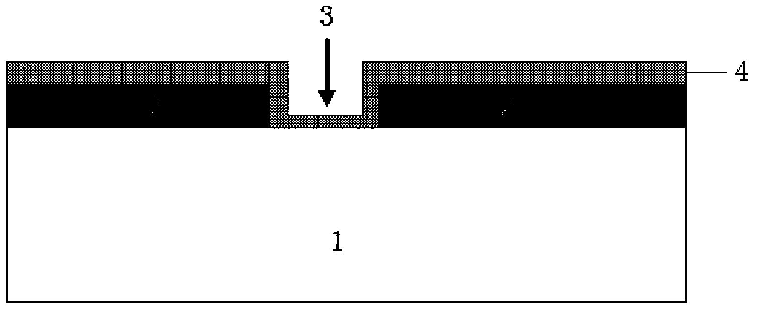
[0025] Step two, combine figure 2 As shown, a metal connection layer 4 is deposited on the pre-metal dielectric layer 2 and in the contact hole 3 . The deposited metal connection layer 4 includes but not limited to titanium, cobalt, tantalum; the thickness of the metal connection layer 4 is The deposition method of the metal connection layer 4 includes but not limited to chemical vapor deposition (CVD) and sputtering.

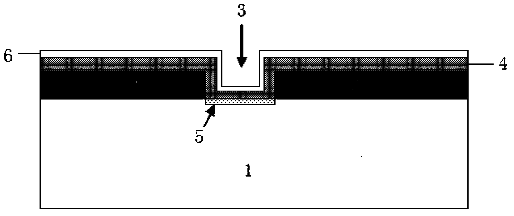
[0026] Step three, combine image 3 As shown, the metal connection layer 4 is subjected to rapid thermal annealing treatment. After the thermal annealing treatment, a metal silic...


PUM


Abstract

The invention discloses a method for improving silicon chip warping degree. The method comprises the following steps: step one: a pre-metal dielectric layer is formed on a silicon substrate, and a contact hole penetrating through the pre-metal dielectric layer is formed in the pre-metal dielectric layer; step two: a layer of metal connecting layer is deposited on the pre-metal dielectric layer and the contact hole; step three: rapid heat annealing processing is performed on the metal connecting layer; step four: plasma etching is performed, and a metal natural oxide layer naturally formed on the surface of the metal connecting layer is removed; and step five: a titanium nitride blocking layer is deposited on the upper surface of the metal connecting layer. Warping degree of silicon chips can be effectively improved by the method so that difficulty in silicon chip production flow is reduced.

Description

technical field [0001] The invention relates to the field of semiconductor integrated circuits, in particular to a method for improving the warpage of silicon wafers. Background technique [0002] In the manufacture of semiconductor power devices and discrete devices, due to the particularity of the front-end process, before the first layer of metal wiring is made, the overall silicon wafer exhibits tensile stress, that is, its warpage is upward warping. [0003] In the existing traditional process method, the first layer of metal wiring is made by first depositing a layer of titanium and titanium nitride as a connection layer and a barrier layer, and then reducing the contact resistance of the contact hole through rapid thermal annealing (that is, reducing The contact resistance between the small titanium and the underlying polysilicon), and then the contact hole is filled, and finally the metal aluminum connection is made. In this traditional process method, if the silico...

Claims


Application Information

Patent Timeline
Patent Type & Authority Applications(China)
IPC IPC(8): H01L21/768
CPCH01L21/76841H01L21/76882
Inventor 成鑫华许升高朱东园
Owner SHANGHAI HUAHONG GRACE SEMICON MFG CORP
Why Eureka
Try Eureka