IGBT capable of realizing localized service lifetime controlling and manufacturing method thereof

A technology for local lifetime control and manufacturing method, which is applied in semiconductor/solid-state device manufacturing, semiconductor devices, electrical components, etc., and can solve problems such as difficulty in achieving local lifetime control, affecting the long-term reliable use of devices, and unfavorable parallel use. Achieve the effect of reducing turn-off tail time, improving anti-latch capability, and precise local life control

Active Publication Date: 2014-03-12
BYD SEMICON CO LTD
View PDF5 Cites 4 Cited by
  • Summary
  • Abstract
  • Description
  • Claims
  • Application Information

AI Technical Summary

Problems solved by technology

[0004] Although this method can increase the turn-off speed of PT-IGBT, the method of electronic irradiation and heavy metal doping lifetime control belongs to global lifetime control, and it is difficult to achieve local lifetime control, such as in figure 1 In the PT-IGBT shown, there is no need for lifetime control near the front PN junctions J1 and J2, but electron irradiation and heavy metal doping will inevitably affect the carrier lifetime here.
An obvious defect of this global lifetime control is that the carrier lifetime of the entire device body region will increase significantly as the temperature rises. When the temperature rises, the carriers stored in the entire n-voltage withstand layer 107 The concentration increases significantly, the on-state voltage drop decreases significantly, and it presents a significant negative temperature coefficient, which is not conducive to parallel use, and the turn-off loss also increases significantly, which affects the long-term reliable use of the device

Method used


Image

  • IGBT capable of realizing localized service lifetime controlling and manufacturing method thereof
  • IGBT capable of realizing localized service lifetime controlling and manufacturing method thereof
  • IGBT capable of realizing localized service lifetime controlling and manufacturing method thereof

Examples


Embodiment Construction

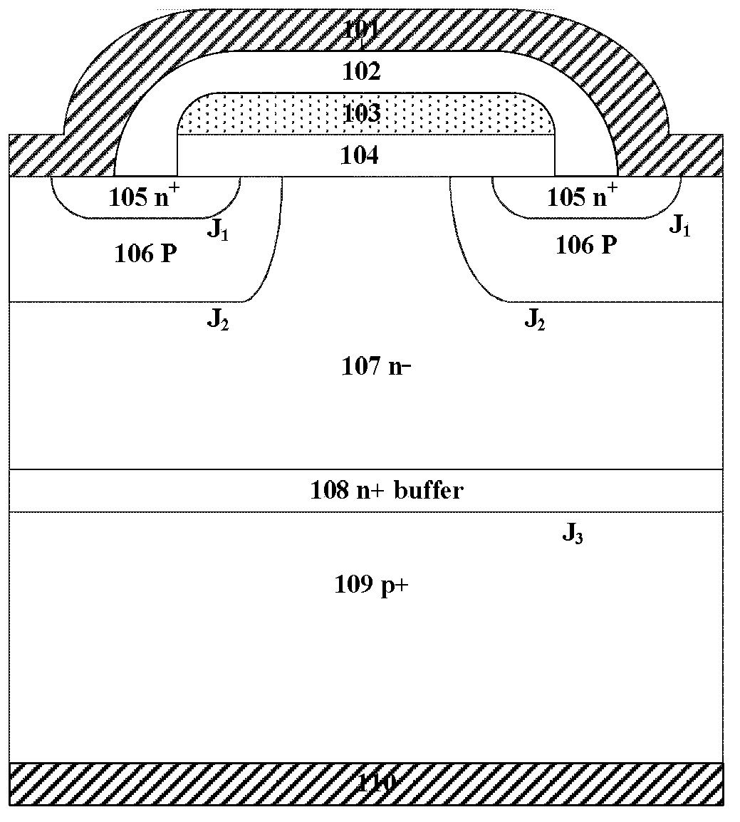
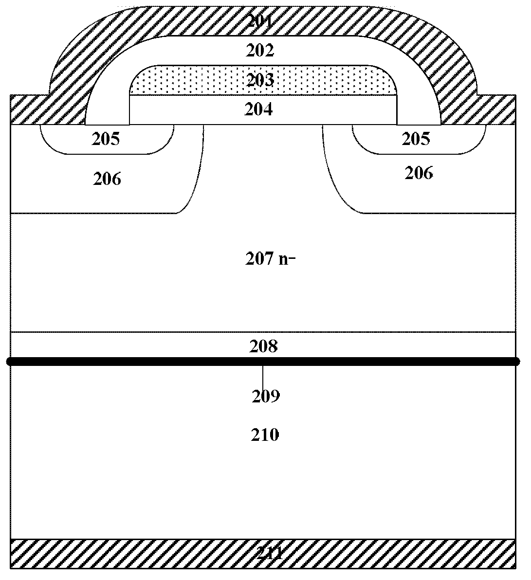
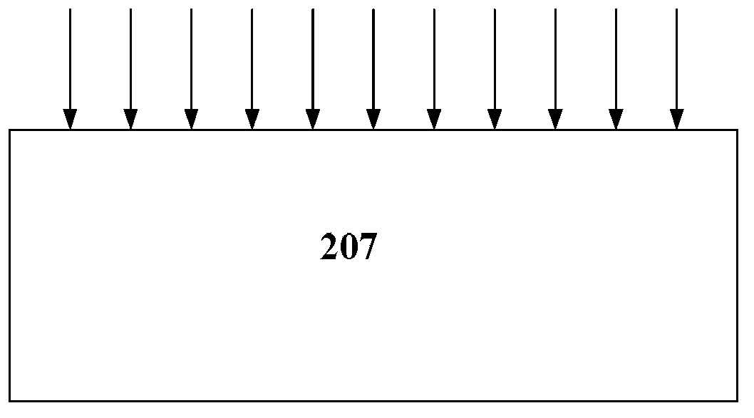
[0057] Embodiments of the present invention are described in detail below, examples of which are shown in the drawings, wherein the same or similar reference numerals designate the same or similar elements or elements having the same or similar functions throughout. The embodiments described below by referring to the figures are exemplary only for explaining the present invention and should not be construed as limiting the present invention.

[0058] In describing the present invention, it should be understood that the terms "longitudinal", "transverse", "upper", "lower", "front", "rear", "left", "right", "vertical", The orientation or positional relationship indicated by "horizontal", "top", "bottom", "inner", "outer", etc. are based on the orientation or positional relationship shown in the drawings, and are only for the convenience of describing the present invention and simplifying the description, rather than Nothing indicating or implying that a referenced device or elem...


PUM


Abstract

The invention brings forward an insulated gate bipolar transistor (IGBT) capable of realizing localized service lifetime controlling and a manufacturing method thereof. The IGBT comprises a current collection region; a buffer layer is formed on the current collection zone; and a drift region is formed on the buffer layer. At least one low-service life high recombination layer is formed between the current collection region and the drift region; and a recombination center is arranged in the low-service life high recombination layer, so that the service life of the carrier is reduced. Besides, well regions are formed in the drift region; emitter regions are formed in the well regions; a gate dielectric layer, a grid electrode and an emitter are successively formed on the drift region; and a collector is formed under the current collection region. According to the invention, because at least one low-service life high recombination layer is formed between the current collection region and the drift region, the low-service life high recombination layer can recombine lots of excess carriers that are generated in a device turn-on state, thereby improving recombination currents and reducing hole injection of the current collection region. Therefore, the turn-off trailing time is shortened; objectives of on-off time reduction and on-off loss reduction can be achieved; and the anti-latch capability of the device is improved.

Description

technical field [0001] The invention belongs to the field of basic electrical components and relates to the preparation of semiconductor devices, in particular to an IGBT structure and a manufacturing method for realizing local lifetime control. Background technique [0002] IGBT (Insulated Gate Bipolar Transistor, Insulated Gate Bipolar Transistor) is a composite voltage-controlled power semiconductor device composed of BJT (Bipolar Transistor) and MOSFET (Insulated Gate Field Effect Transistor). It has the main advantages of power BJT and power MOSFET: high input impedance, small input driving power, small on-resistance, large current capacity, fast switching speed, etc. In this era of high-voltage and high-frequency power electronic devices, IGBT has undoubtedly become the mainstream device in the field of power electronics applications. The development of IGBT has roughly experienced three generations of technology: PT-IGBT (punch-through IGBT), NPT-IGBT (non-punch-thro...

Claims


Application Information

Patent Timeline
Patent Type & Authority Applications(China)
IPC IPC(8): H01L29/739H01L29/06H01L21/331
CPCH01L29/1095H01L29/66333H01L29/7396
Inventor 吴海平秦博肖秀光
Owner BYD SEMICON CO LTD
Why Eureka
Try Eureka