Common wiring microelectrode array chip and manufacturing method thereof
A micro-electrode array and co-wiring technology, applied in the field of cell micro-electrode array chip and its preparation, can solve the problem of single use, etc., and achieve the effects of excellent conductivity, novel structure and high sensitivity
- Summary
- Abstract
- Description
- Claims
- Application Information
AI Technical Summary
Problems solved by technology
Method used
Image

Examples
Embodiment
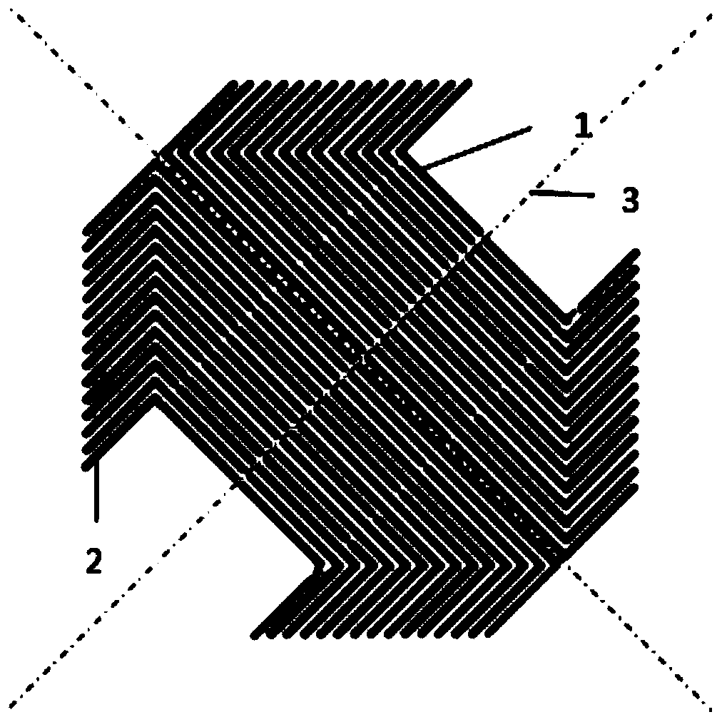
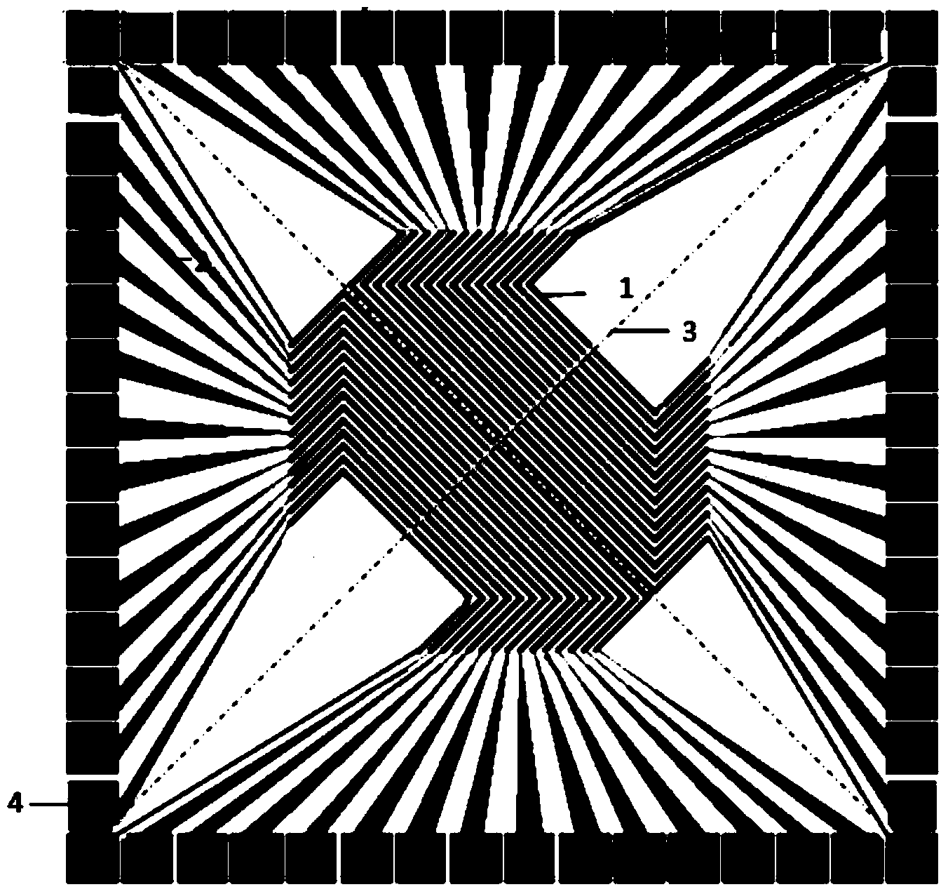
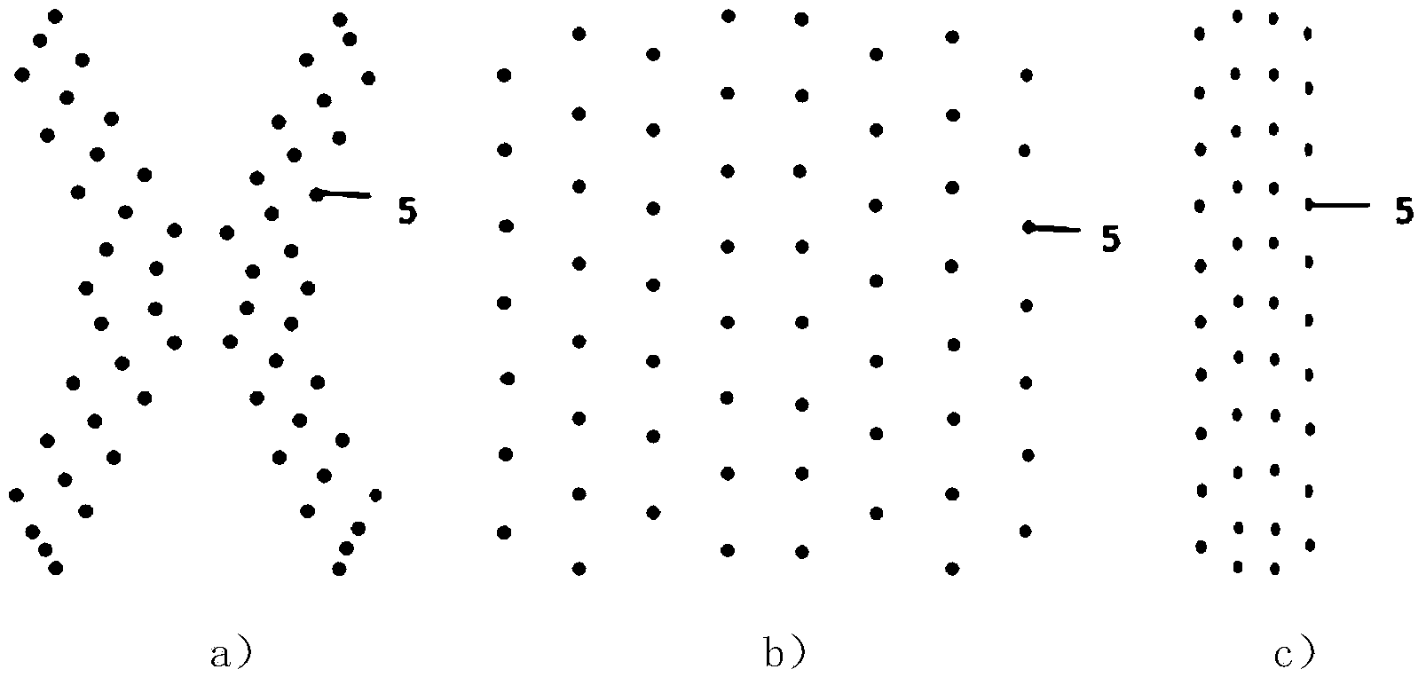
[0034] This embodiment relates to a co-wiring micro-electrode array chip, its structure is as follows Figure 4 As shown, the microelectrode array structure layer on the chip includes a plurality of microelectrodes 1 arranged in a grating array structure and a plurality of microelectrodes 5 arranged in a dot-like array structure superimposed on the grating array.
[0035] The co-wiring microelectrode array chip of this embodiment adopts a new structural design and process, specifically: designing a first mask with a grating array structure and a second mask with a dot matrix array structure in a certain arrangement ; Deposit a layer of metal on the glass substrate, use the first mask, and use photolithography technology to prepare the grating array electrode with the required photoresist structure; use the mask of photoresist and metal, and use ion beam etching technology , open a metal window to obtain a grating electrode array chip; then deposit SiO on the chip in turn 2The...
PUM
| Property | Measurement | Unit |
|---|---|---|
| width | aaaaa | aaaaa |
| length | aaaaa | aaaaa |
| thickness | aaaaa | aaaaa |
Abstract
Description
Claims
Application Information
 - R&D Engineer
- R&D Manager
- IP Professional
- Industry Leading Data Capabilities
- Powerful AI technology
- Patent DNA Extraction
Browse by: Latest US Patents, China's latest patents, Technical Efficacy Thesaurus, Application Domain, Technology Topic.
© 2024 PatSnap. All rights reserved.Legal|Privacy policy|Modern Slavery Act Transparency Statement|Sitemap