A method of manufacturing a fin field effect transistor

A field effect transistor and fin technology, which is applied in the field of fin field effect transistor preparation, can solve the problems of difficulty in controlling the height of the fin, affecting the performance of the fin field effect transistor, etc., and achieves easy control of the aspect ratio of the fin and easy height difference. The effect of controlling and improving yield

Active Publication Date: 2016-09-21
SEMICON MFG INT (SHANGHAI) CORP +1
View PDF7 Cites 0 Cited by
  • Summary
  • Abstract
  • Description
  • Claims
  • Application Information

AI Technical Summary

Problems solved by technology

[0004] At present, it is difficult to control the height of the fins in the manufacturing process of the fin field effect transistor, and the existing preparation methods cannot solve this problem well, which affects the performance of the fin field effect transistor

Method used


Image

  • A method of manufacturing a fin field effect transistor
  • A method of manufacturing a fin field effect transistor
  • A method of manufacturing a fin field effect transistor

Examples


Embodiment approach

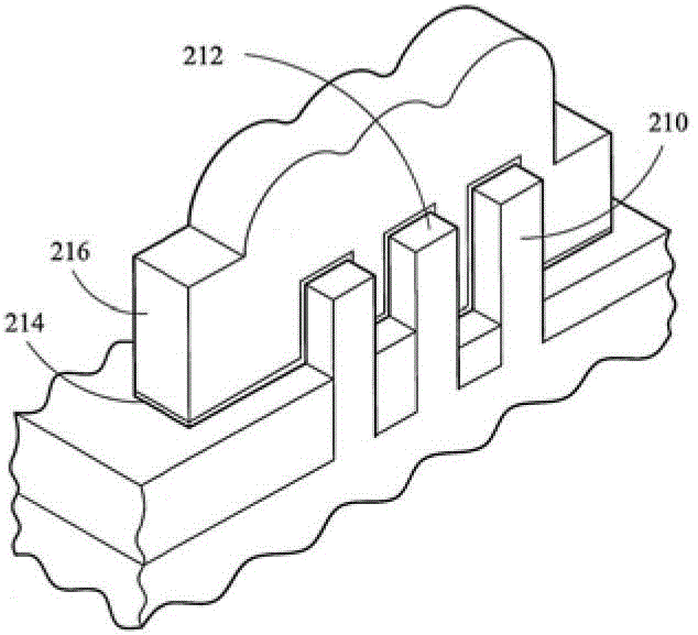
[0040] According to the flow chart, the present invention can have the following two implementations, which will be described separately below, first referring to Figure 2-7 Explain the first case:

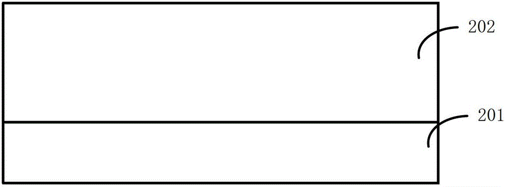
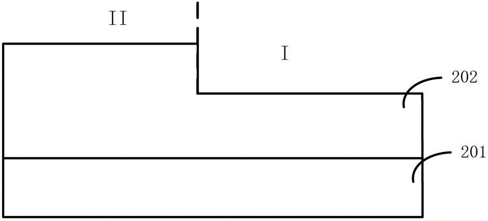
[0041] refer to figure 2 Firstly, a semiconductor substrate 201 is provided, and the semiconductor substrate may be at least one of the materials mentioned below: silicon, Ge or SiGe and the like.

[0042]An isolation structure may also be formed in the semiconductor substrate, and the isolation structure is a shallow trench isolation (STI) structure or a local oxide of silicon (LOCOS) isolation structure. In the present invention, shallow trench isolation is preferably formed, and various well structures and channel layers on the substrate surface are also formed in the semiconductor substrate. Generally speaking, the conductivity type of ion doping forming the well structure is the same as that of the channel layer, but the concentration is lower than that of the gate channe...


PUM


Abstract

The invention relates to a fin field effect transistor preparation method. The preparation method comprises the following steps: a base is provided, wherein the base comprises a semiconductor substrate and an insulating layer located on the semiconductor substrate, the base has a stepped shape and has a high region and a low region; a hard mask layer is formed on the insulating layer and planarization is performed; the hard mask layer and the insulating layer are etched, and at least one groove is formed in the high region and the low region of the base separately so as to expose the semiconductor substrate; the groove is filled with a semiconductor material and planarization is performed to form a fin pattern; and the hard mask layer is removed through etching to form fins having different heights. According to the invention, the heights of the fins, the height difference of the fins having different heights and the fin depth-width ratio can be controller easier, the problem that the fin height is not easy to control in the prior art can be solved skillfully, and the yield of semiconductor devices can be improved.

Description

technical field [0001] The invention relates to the field of semiconductors, and in particular, the invention relates to a method for preparing a fin field effect transistor. Background technique [0002] The improvement of integrated circuit performance is mainly achieved by continuously shrinking the size of integrated circuit devices to increase its speed. Currently, as the semiconductor industry has advanced to nanotechnology process nodes in pursuit of high device density, high performance, and low cost, manufacturing and design challenges have led to the development of three-dimensional designs such as Fin Field Effect Transistors (FinFETs). Typical FinFETs are fabricated using thin vertical "fins" (or fin structures) extending from a substrate formed, eg, by etching away a portion of the silicon layer. A FinFET channel is formed in the vertical fin, a surrounding gate is formed above the fin, and the channel is controlled from both sides through the gate. Additional...

Claims


Application Information

Patent Timeline
Patent Type & Authority Patents(China)
IPC IPC(8): H01L21/336
Inventor 鲍宇
Owner SEMICON MFG INT (SHANGHAI) CORP
Why Eureka
Try Eureka