Schottky diode chip, Schottky diode device and manufacturing method for Schottky diode chip-composite barrier

A technology of Schottky diodes and chips, which is applied in the direction of diodes, semiconductor/solid-state device manufacturing, semiconductor devices, etc., can solve the problems of inability to effectively adjust the barrier height, reduce the fatigue resistance of devices, and weak barrier diffusion, and meet the requirements of High temperature performance, improved fatigue resistance, and low cost effects

Active Publication Date: 2014-03-26
济南市半导体元件实验所
View PDF9 Cites 16 Cited by
  • Summary
  • Abstract
  • Description
  • Claims
  • Application Information

AI Technical Summary

Problems solved by technology

However, this process and the resulting device also have the following disadvantages: 1. A single metal molybdenum is selected as the barrier metal, which cannot effectively adjust the height of the barrier and balance the contradiction between the forward and reverse characteristics. The ability to withstand voltage, burnout, and antistatic needs to be improved, and it is easy to burn out when used in a high-temperature environment; 2. Titanium is selected as a diffusion barrier. Although titanium metal has strong adhesion, it has high activity and a weak barrier to diffusion. , which reduces the anti-fatigue performance of the device; 3. Under high current density, the anti-electromigration performance is poor

Method used


Image

  • Schottky diode chip, Schottky diode device and manufacturing method for Schottky diode chip-composite barrier
  • Schottky diode chip, Schottky diode device and manufacturing method for Schottky diode chip-composite barrier

Examples


Embodiment 1

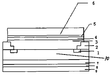
[0045] The power Schottky device of the present invention such as figure 1 As shown, there is a semiconductor substrate 10, the substrate is an N-type silicon chip, and the front side of the semiconductor substrate is provided with a silicon dioxide oxide layer 2, and the middle part of the oxide layer has a window, and the longitudinal section of the window is T shape, so that the side of the oxide layer with a window is stepped, and a barrier layer 3 is provided in the window. The barrier layer covers the mesa of the oxide layer and extends to the highest surface of the oxide layer. The material of the barrier layer is NiPtSi , the potential barrier layer is in direct contact with the semiconductor substrate to form a NiPtSi-Si potential barrier, the front multilayer metal electrode is arranged on the potential barrier layer, and the back multilayer metal electrode is arranged on the back of the semiconductor substrate. A guard ring 1 is also provided in the semiconductor s...

Embodiment 2

[0052] The preparation method of the power Schottky device composite barrier of the present invention comprises the following steps:

[0053] (1) Oxidation: Oxidize the silicon wafer to form an oxide layer SiO2 on its surface;

[0054] (2) Perform a photolithography on the silicon wafer to form an annular groove window on the oxide layer. The longitudinal section of the window is T-shaped. The surface of the oxide layer after photolithography is flat. , the height of the mesa is lower than the height of the surface of the oxide layer, so that the window side of the oxide layer annular groove has a stepped edge;

[0055] (3) Boron diffusion: the boron diffusion method of solid flake BN is used to make a protective ring on the silicon wafer;

[0056] (4) Main diffusion: Use a high temperature of 1100°C to carry out deep advancement of the guard ring junction, and the time is about 1h;

[0057] (5) Carry out secondary photolithography to form barrier region windows;

[0058] (...


PUM

PropertyMeasurementUnit
thicknessaaaaaaaaaa
thicknessaaaaaaaaaa

Abstract

The invention discloses a Schottky diode chip, a Schottky diode device and a manufacturing method for a Schottky diode chip-composite barrier. The Schottky diode chip comprises an N-type silicon semiconductor substrate; the obverse side of the semiconductor substrate is provided with a NiPtSi barrier layer, and the barrier layer makes direct contact with the semiconductor substrate to form a NiPtSi-Si barrier. The manufacturing method is simple, low in cost, practical and effective; NiPt alloy is adopted as Schottky barrier metal, and the composite metal silicide-silicon contact barrier (NiPtSi-Si) is formed; the obtained chip and the device eliminate the contradiction between forward voltage drop and reverse electric leakage with regard to a single-metal barrier, the reverse electric leakage and the forward voltage drop are both low, and meanwhile high-temperature resistant performance, antistatic performance, reverse energy impact performance and the like are well improved.

Description

technical field [0001] The invention particularly relates to a preparation process of a composite metal silicide / silicon contact composite barrier and a Schottky diode chip and device containing the composite barrier, which are key core technologies for manufacturing Schottky barrier devices. Background technique [0002] Power Schottky diodes are manufactured using the principle of metal-semiconductor junctions formed by metal-semiconductor contacts. The electrical parameters of power Schottky devices mainly include: forward voltage drop, reverse voltage, reverse leakage, etc. It is a low-power, ultra-high-speed semiconductor device. It is mostly used as a high-frequency, low-voltage, high-current rectifier diode, freewheeling diode, and protection diode. It is also useful as a rectifier diode and small-signal detector diode in microwave communication circuits. It is common in communication power supplies, inverters, smart phones, etc. In order to balance the contradicti...

Claims


Application Information

Patent Timeline
Patent Type & Authority Applications(China)
IPC IPC(8): H01L29/872H01L21/329H01L29/24
CPCH01L29/24H01L29/66212H01L29/872
Inventor 陈守迎董军单维刚杨晓亮沈中堂宋迎新
Owner 济南市半导体元件实验所
Why Eureka
Try Eureka