A method for preparing nanoscale spherical structures on the surface of light-emitting diodes
A light-emitting diode and nanoscale technology, applied in semiconductor devices, electrical components, circuits, etc., can solve the problems of inability to effectively control the shape, size and period of the roughened structure, and the inability to prepare periodic convex and concave ball structures with extraction efficiency
- Summary
- Abstract
- Description
- Claims
- Application Information
AI Technical Summary
Problems solved by technology
Method used
Image
Examples
Embodiment 1
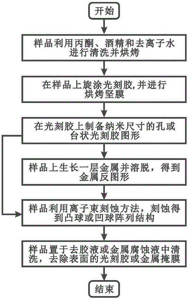
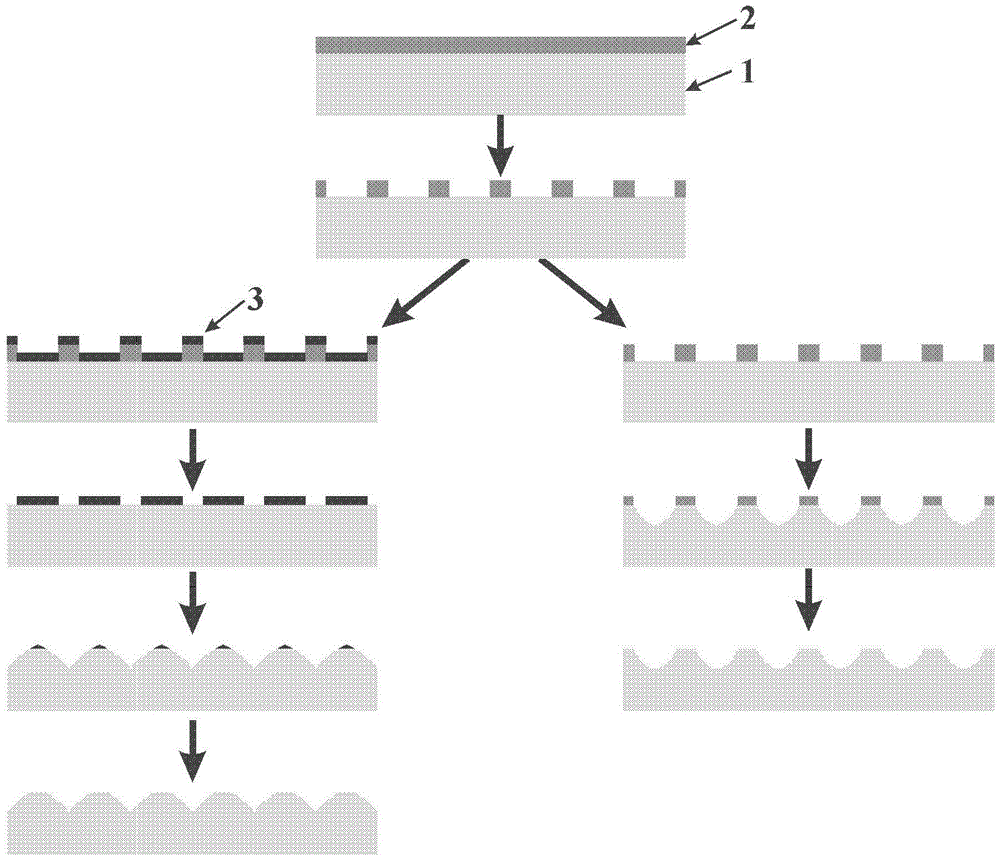
[0038] Embodiment 1: The method for preparing periodic convex ball and concave ball structures for LED luminous efficiency enhancement on the surface of LED chip or substrate provided by the present invention comprises the following steps:
[0039] Step 1) Cleaning of LED chips: Clean the LED chips to be patterned accordingly, and then bake the cleaned chips (or samples) on a hot plate, for example, on a hot plate with a temperature of 150°C 10 minutes to remove the water on the chip surface;
[0040] Step 2) Coating of photoresist: Put the chip cleaned in step 1) into the coating machine, and apply the photoresist by spin coating, select different photoresist according to the exposure type, After the photoresist is spin-coated, it is baked using a hot plate or an oven, and the temperature of the baking is determined by the type of photoresist.
[0041] Step 3) Preparation of photoresist nanopatterns: the chip coated with photoresist in step 2) is prepared for nanopatterns, f...
Embodiment 2
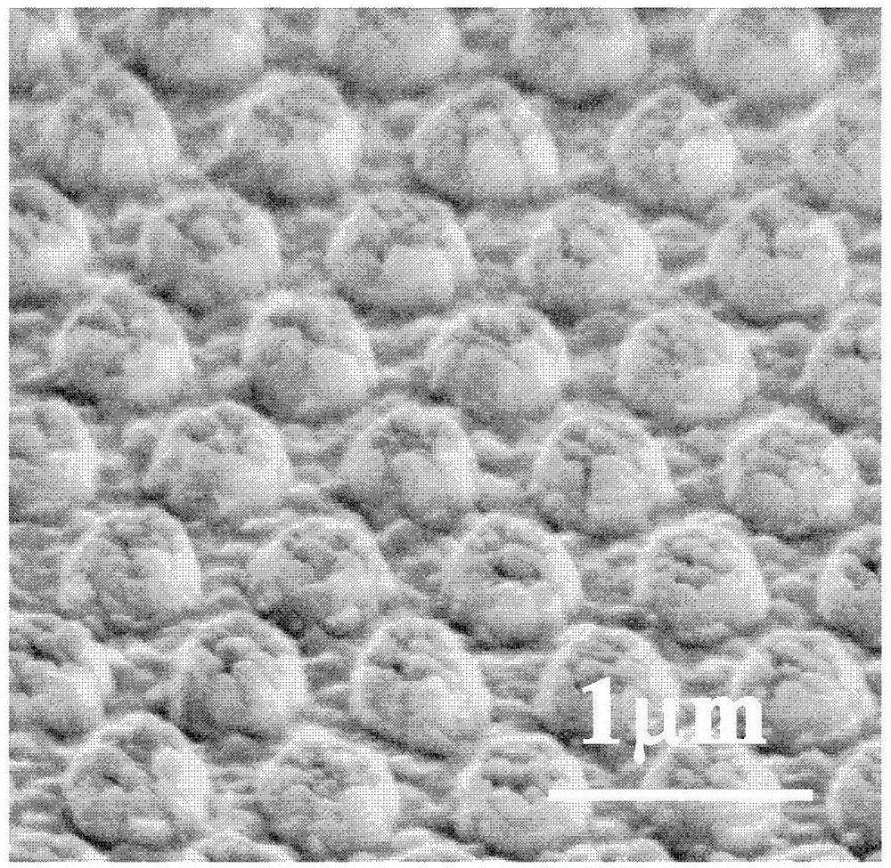
[0045] Embodiment 2: Utilizing the preparation method of the present invention, adopting electron beam exposure and metal coating stripping to make a metal mask, etching on the ITO layer of the formal LED to realize the convex ball structure, specifically including the following steps:
[0046] Step 1) The LED chip to be fabricated is cleaned by ultrasonic cleaning in three steps of acetone, alcohol and secondary deionized water, each step is cleaned for 5 minutes, and finally baked on a hot plate at 150° C. for 10 minutes.
[0047] Step 2) The electron beam photoresist PMMA is spin-coated on the LED chip, and the sample is baked on a hot plate at 180° C. for 1 minute after spin-coating.
[0048] Step 3) preparing a circular hole array photoresist pattern with a diameter of 400nm and a period of 750nm on the photoresist by electron beam exposure;
[0049] Step 4) putting the chip prepared in step 3) into a thermal evaporation device to grow a metal chromium film with a thickne...
Embodiment 3
[0053] In this embodiment, the photoresist pattern is prepared by nanoimprinting method, and the photoresist is used as a mask to etch the ITO layer of the formal LED to realize the concave ball structure, which specifically includes the following steps:
[0054] Step 1) The LED substrate to be fabricated is cleaned by ultrasonic cleaning in three steps of acetone, alcohol and secondary deionized water, each step is cleaned for 5 minutes, and finally baked on a hot plate at 150° C. for 10 minutes.
[0055] Step 2) Spin-coat the nano-imprint adhesive PMMA on the LED sample, and bake the sample on a hot plate at 180° C. for 1 minute after spin-coating.
[0056] Step 3) using the nanoimprint process to prepare a circular hole array pattern with a diameter of 200nm and a period of 450nm on the glue;
[0057] Step 4) Place the sample obtained in step 3) on the sample stage of the ion beam etching system, adjust the ion energy to 300eV, the beam current density to 0.8mA / cm2, the sam...
PUM
 Abstract
Description
Claims
Application Information
 - R&D
- Intellectual Property
- Life Sciences
- Materials
- Tech Scout
- Unparalleled Data Quality
- Higher Quality Content
- 60% Fewer Hallucinations
Browse by: Latest US Patents, China's latest patents, Technical Efficacy Thesaurus, Application Domain, Technology Topic, Popular Technical Reports.
© 2025 PatSnap. All rights reserved.Legal|Privacy policy|Modern Slavery Act Transparency Statement|Sitemap|About US| Contact US: help@patsnap.com


