Large-area manufacturing method and processing system for surfaces of micrometer and nanometer structures with tunable periods and tunable morphologies

A technology of micro-nano structure and processing system, which is applied in the field of large-area preparation method and processing system of micro-nano structure surface with tunable periodic morphology, which can solve the problem of poor tunability, single micro-nano structure morphology, and difficulty in meeting multi-functional surfaces. Processing requirements and other issues, to achieve the effect of simple device and flexible control

Active Publication Date: 2014-04-09
UNIV OF SCI & TECH OF CHINA
View PDF11 Cites 21 Cited by
  • Summary
  • Abstract
  • Description
  • Claims
  • Application Information

AI Technical Summary

Problems solved by technology

[0004] However, the limitation of the laser interference processing method is that it can only generate an interference field with a fixed period and light intensity distribution, and the resulting micro-nano structure has a single morphology and poor tunability, which makes it difficult to meet the processing requirements of a specially designed multifunctional surface.
In practical applications, large-area non-periodic (or gradually changing periodic) sub-micron fine structures are required in many cases, which poses a challenge to traditional interference processing technology

Method used


Image

  • Large-area manufacturing method and processing system for surfaces of micrometer and nanometer structures with tunable periods and tunable morphologies
  • Large-area manufacturing method and processing system for surfaces of micrometer and nanometer structures with tunable periods and tunable morphologies
  • Large-area manufacturing method and processing system for surfaces of micrometer and nanometer structures with tunable periods and tunable morphologies

Examples


Embodiment 1

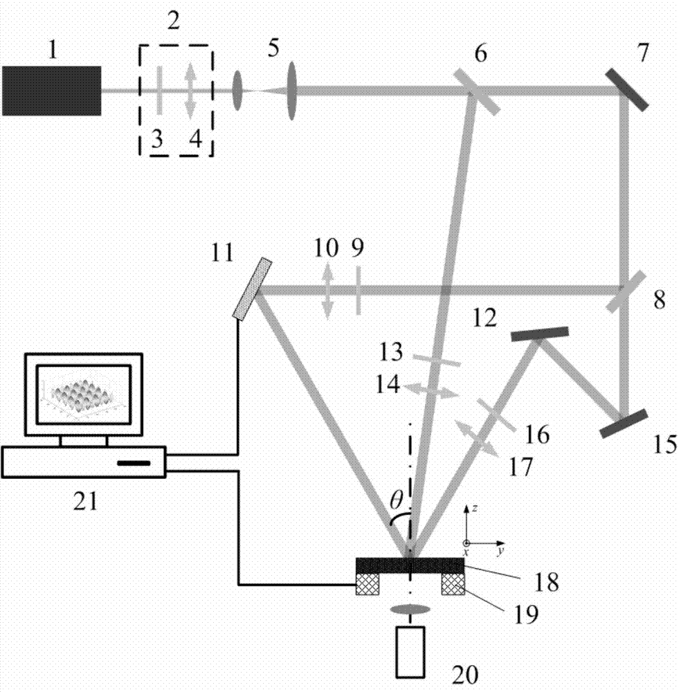
[0046] The wavefront control laser interference processing system includes a laser light source 1, an energy attenuator 2, a beam expander 5, first, second, and third mirrors 7, 12, 15, first, and second beam splitters 6, 8, First, second, third, fourth half-wave plates 3, 9, 13, 16, first, second, third, fourth polarizers 4, 10, 14, 17, wavefront modulation device 11, CCD camera 20, precision mobile platform 19 and computer 21, such as figure 1shown. The half-wave plate and polarizer are used to control the energy and polarization state of each beam; the wavefront modulation device is used to regulate the wavefront of the spatial beam; the precision mobile platform is used to position and move the sample; the CCD camera is used to monitor the process and detect Processing results. The energy of the laser beam emitted by the laser light source 1 is adjusted to an appropriate value through the energy attenuator 2, wherein the energy attenuator 2 includes the first half-wave p...

Embodiment 2

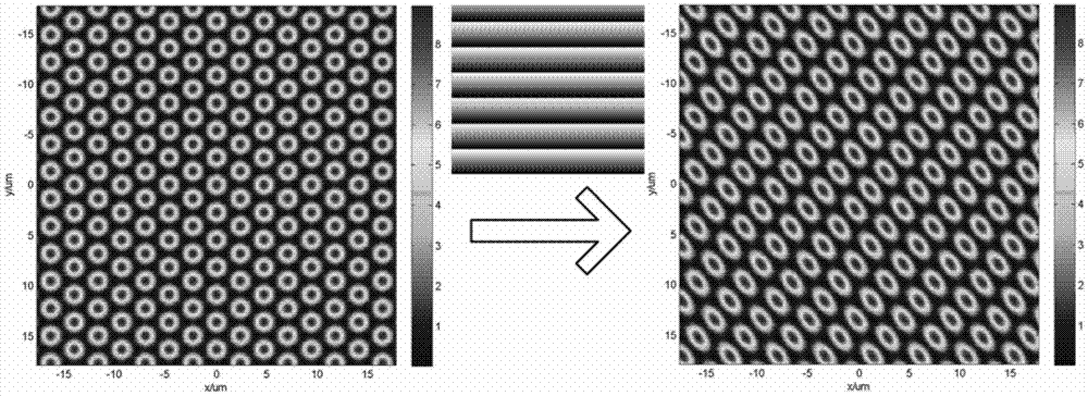
[0050] The laser light source 1 is selected as a nanosecond pulsed laser with a wavelength of 355nm, the outgoing light is divided into three beams and one of them is purely phase-modulated by the deformable mirror 11 ( figure 1 ). The three beams of light are evenly distributed in space, their azimuth angles are all 5°, and their polar angles are (0°, 120°, 240°). The polarization directions of the three light beams are (-30°, 135°, 300°) in turn. When the three beams of spatial light are not phase-modulated, the interference pattern is a uniformly distributed rectangular intensity peak ( image 3 ). When using the deformable mirror 11 to apply a one-dimensional sinusoidal grating ( image 3 ) phase modulation, the interference image is modulated into a non-uniform diamond-shaped intensity peak ( image 3 ), which can be used for photolithographic processing of non-periodic arrays.

Embodiment 3

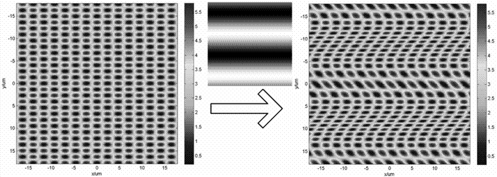
[0052] The laser light source 1 is selected as a nanosecond pulsed laser with a wavelength of 355nm, the outgoing light is divided into three beams and one of them is amplitude modulated by a digital micromirror array 11 ( figure 1 ). The three beams of light are evenly distributed in space, their azimuth angles are all 5°, and their polar angles are (0°, 120°, 240°). The polarization directions of the three beams are (-30°, 210°, 450°) in sequence. When the amplitude modulation of the three beams of spatial light is not performed, the interference pattern is a uniformly distributed circular Gaussian distribution of intensity valleys ( Figure 4 ). When using the digital micromirror array 11 to apply a pattern type ( Figure 4 ) amplitude modulation, the interference image is modulated to pattern-limited intensity valleys ( Figure 4 ), which can be used for photolithographic processing of maskless patterned periodic arrays.


PUM

PropertyMeasurementUnit
wavelengthaaaaaaaaaa

Abstract

The invention discloses a large-area manufacturing method and a processing system for the surfaces of micrometer and nanometer structures with tunable periods and tunable morphologies. A laser interference processing method is a widely applied micrometer and nanometer processing means, but is limited and only can be used for realizing intensity distribution of interference fields with fixed periods and fixed morphologies, accordingly, micrometer and nanometer structures processed by the laser interference processing method have single morphologies and are poor in tenability, and requirements on processing multifunctional surfaces in specific designs cannot be met. The large-area manufacturing method and the processing system have the advantages that the large-area manufacturing method and the processing system aim to overcome the bottleneck of the traditional laser interference processing technology, a wave-front modulation device is used for precisely controlling wave-front phases and vibration amplitudes of beams on the basis of the original multi-beam laser interference processing system, so that preliminarily designed target intensity distribution of interference light fields can be realized, and the large-area micrometer and nanometer structures with the variable periods and the variable morphologies can be finally processed; an effective way can be provided for manufacturing the large-area surfaces of non-periodic and diversified structures on a large scale.

Description

technical field [0001] The invention belongs to the technical field of micromachining, and in particular relates to a large-area preparation method and a processing system of a micro-nano structured surface with tunable periodic morphology. Background technique [0002] Laser processing technology is an important micro-nano processing method. Through the interaction between light and materials, it can produce controllable micro-nano structures on the surface of materials. Laser processing technology has the advantages of high efficiency, simplicity, green and pollution-free. Laser processing methods can be mainly divided into direct writing processing and interference processing. Laser direct writing processing technology can prepare fine structures with arbitrary shapes, but the processing process is time-consuming and inefficient, making it difficult to be used in mass production. The laser interference processing method acts on the material through the space-time super...

Claims


Application Information

Patent Timeline
Patent Type & Authority Applications(China)
IPC IPC(8): B23K26/067
CPCB23K26/0673
Inventor 胡衍雷黄文浩李家文褚家如
Owner UNIV OF SCI & TECH OF CHINA
Why Eureka
Try Eureka