
Iii-nitride metal insulator semiconductor field effect transistor

A technology of field effect transistors and nitrides, applied in semiconductor devices, semiconductor/solid-state device manufacturing, electrical components, etc.

Active Publication Date: 2014-04-09
HRL LAB
View PDF4 Cites 6 Cited by
  • Summary
  • Abstract
  • Description
  • Claims
  • Application Information

AI Technical Summary

Problems solved by technology

As discussed above, despite many years of research, it has not been successful to achieve both low gate leakage current and low interfacial trap density as shown by threshold voltage hysteresis, maximum drain current density and off-state drain leakage current, especially in normally closed transistor

Method used


Image

  • Iii-nitride metal insulator semiconductor field effect transistor
  • Iii-nitride metal insulator semiconductor field effect transistor
  • Iii-nitride metal insulator semiconductor field effect transistor

Examples


Embodiment Construction

[0019] In the following description, numerous specific details are set forth in order to clearly describe various embodiments disclosed herein. However, it will be understood by those skilled in the art that the present invention may be practiced without the specific details discussed below. In other instances, well-known features have not been described in order not to obscure the invention.

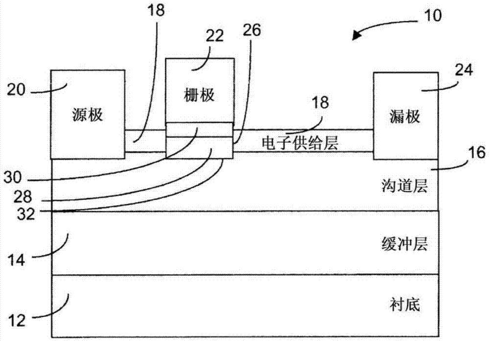
[0020] figure 1 An elevational cross-sectional view of a FET 10 device structure according to the present invention is shown. The FET has a buffer layer 14 formed on a substrate 12 . A channel layer 16 is formed on the buffer layer 14 , and an electron supply layer 18 , which may also be referred to as a barrier layer, is formed on the channel layer 16 .

[0021] The material of the substrate 12 may be silicon (Si), silicon carbide (SiC), sapphire, gallium nitride (GaN), or aluminum nitride (AlN).

[0022] The buffer layer 14 may be a stack of III-nitride materials grown on the subs...


PUM

PropertyMeasurementUnit
Thicknessaaaaaaaaaa
Layer thicknessaaaaaaaaaa
Thicknessaaaaaaaaaa

Abstract

A field effect transistor (FET) includes a Ill-Nitride channel layer, a III -Nitride barrier layer on the channel layer, wherein the barrier layer has an energy bandgap greater than the channel layer, a source electrode electrically coupled to one of the Ill-Nitride layers, a drain electrode electrically coupled to one of the Ill- Nitride layers, a gate insulator layer stack for electrically insulating a gate electrode from the barrier layer and the channel layer, the gate insulator layer stack including an insulator layer, such as SiN, and an AlN layer, the gate electrode in a region between the source electrode and the drain electrode and in contact with the insulator layer, and wherein the AlN layer is in contact with one of the III- Nitride layers.

Description

[0001] Cross References to Related Applications [0002] This application claims priority to US Provisional Application No. 61 / 513426, filed July 29, 2011, which is incorporated herein by reference in its entirety. This application is related to US Patent Application No. 12 / 909,497, filed October 21, 2010, which was issued as US Patent No. 8,124,505 on February 28, 2012. technical field [0003] The present invention relates to a III-nitride field effect transistor (FET), in particular to [0004] Device structure and fabrication method of Metal Insulator Semiconductor Field Effect Transistor. Background technique [0005] Due to the excellent material properties of GaN, transistors fabricated from it are suitable for high voltage, high temperature and high speed operation. A key application of GaN transistors is in the fabrication of switching devices capable of controlling the flow of electrical power. For power switching applications, there is a strong demand to use no...

Claims


Application Information

Patent Timeline
IPC IPC(8): H01L29/772H01L21/335
CPCH01L29/7787H01L29/2003H01L29/4236H01L29/513H01L29/66462H01L29/66522H01L29/7786H01L29/78H01L29/2006H01L29/205
Inventor 储荣明大卫·F·布朗陈旭亚当·J·威廉姆斯卡里姆·S·保特罗斯
Owner HRL LAB
Features
  • Generate Ideas
  • Intellectual Property
  • Life Sciences
  • Materials
  • Tech Scout
  • Unparalleled Data Quality
  • Higher Quality Content
  • 60% Fewer Hallucinations
Learn More