Method for making micro-nano-scale pattern embossing mold

A production method and pattern technology are applied in the production of micro-nano-scale pattern imprinting molds and the fields of imprinting and imprinting molds, which can solve the problems of slow speed of high-precision patterns, unsuitable for large-area nanostructure production, and insufficiently fine stripe scales. , to achieve the effect of improving anti-counterfeiting ability, low cost and large format

Active Publication Date: 2016-06-29
HUAZHONG UNIV OF SCI & TECH
View PDF4 Cites 0 Cited by
  • Summary
  • Abstract
  • Description
  • Claims
  • Application Information

AI Technical Summary

Problems solved by technology

[0007] The invention provides a method for making a micro-nano-scale pattern imprinting mold, which solves the problem that the stripe scale of the imprinting mold made by laser interference lithography is not fine enough, and the speed of making high-definition patterns by electron beam lithography is too slow, which is not suitable for large-area nanostructures. production problem

Method used


Image

  • Method for making micro-nano-scale pattern embossing mold
  • Method for making micro-nano-scale pattern embossing mold
  • Method for making micro-nano-scale pattern embossing mold

Examples


Embodiment 1

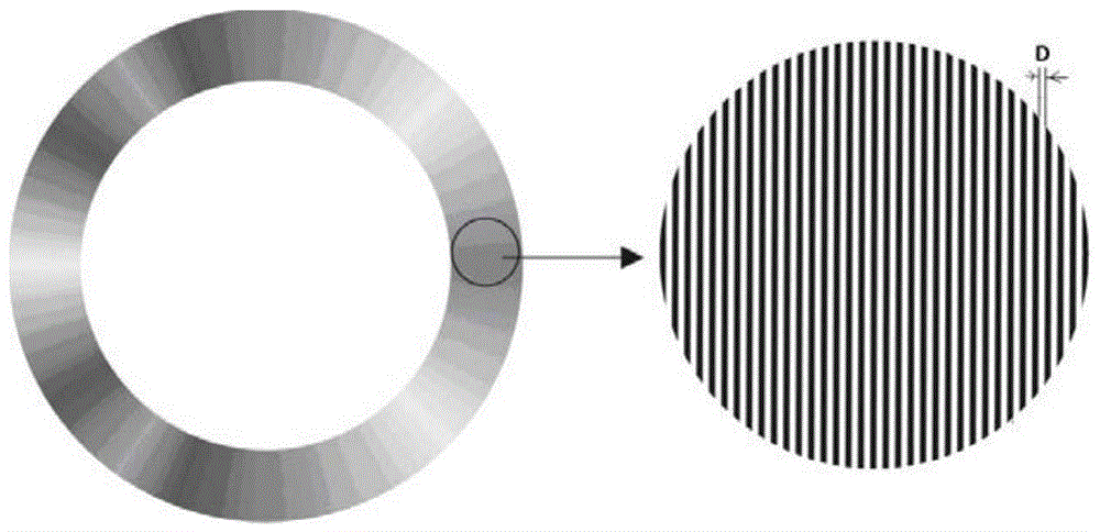
[0047] Embodiment 1: as image 3 As shown, the sequence includes the following steps:

[0048] (1) Electron beam lithography step;

[0049] First, spin-coat ZEP520 electronic glue with a thickness of 400nm on the silicon substrate, and then use electron beam exposure to make nano-sized patterns of grating structures as shown in Figure 2(b) and Figure 2(c), develop and fix Finally, a nanometer-sized pattern with a line width of 200nm is obtained on the silicon substrate;

[0050] (2) a dry etching step;

[0051] Use the remaining electronic glue as a mask, and dry-etch the silicon substrate to obtain a nano-sized pattern with a depth of 100nm and a line width of 200nm;

[0052] (3) laser interference lithography step;

[0053] Clean and remove the remaining electronic glue, spin-coat AZ3100 photoresist with a thickness of 1500nm on the surface of the silicon substrate, and then make a photoresist on the adjacent part or surrounding part of the corresponding nanometer-sized ...

Embodiment 2

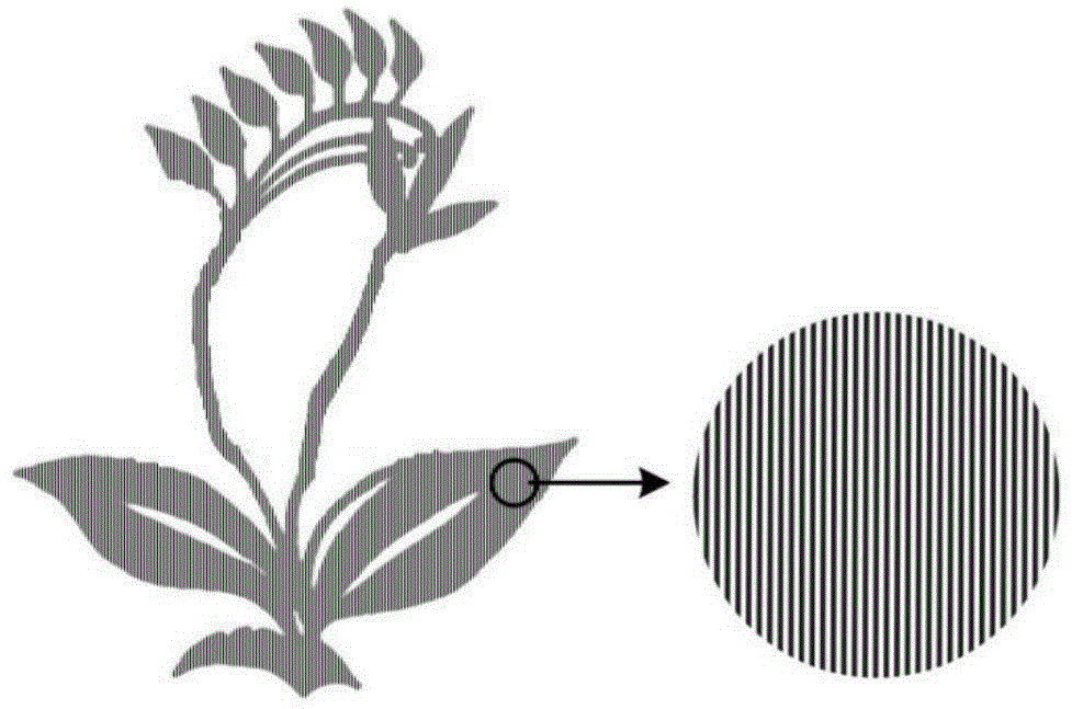
[0061] Example 2, such as Figure 4 As shown, the sequence includes the following steps:

[0062] (1) laser interference lithography step;

[0063] Spin-coat AZ3100 photoresist with a thickness of 1500nm on the surface of the silicon substrate, and then make a micro-nano-sized pattern on the photoresist as shown in Figure 2(a), and use laser interference to photoetch the micro-nano-sized pattern , after developing and fixing, a micro-nano-sized pattern with a line width of 600nm is obtained on the silicon substrate;

[0064] (2) a dry etching step;

[0065] Using the remaining photoresist as a mask, dry-etch the silicon substrate to obtain micro-nano-sized patterns with a depth of about 300nm and a line width of 600nm;

[0066] (3) Electron beam lithography step;

[0067] Clean and remove the remaining photoresist on the silicon substrate, spin-coat ZEP520 electronic glue with a thickness of 400nm on the silicon substrate, and make it on the electronic glue corresponding t...


PUM

PropertyMeasurementUnit
depthaaaaaaaaaa
widthaaaaaaaaaa
depthaaaaaaaaaa

Abstract

The invention discloses methods for manufacturing a micro / nano scale pattern stamping die to solve the problems that a laser interference photo-etched die is not exquisite enough in pattern scale, the speed is too low when high-precision patterns are manufactured through electron beam photo-etching, and the electron beam photo-etching is not suitable for large-area manufacture, and belongs to stamping die finish machining methods. One of the methods sequentially includes the steps of electron beam photo-etching, primary dry etching, laser interference etching, secondary dry etching, nanometer stamping and micro-electroforming. The other method sequentially includes the steps of laser interference etching, primary dry etching, electron beam etching, secondary dry etching, nanometer stamping and micro-electroforming. The advantage that electron beam etching is exquisite in manufacture and the advantages that the laser interference etching is low in cost and large in width of a manufactured die are combined, nano scale patterns and micro scale patterns are manufactured at different positions of the stamping die, the expressive force of the manufactured patterns is far better than the expressive force of patterns manufactured through traditional laser interference etching, and the anti-counterfeiting capacity of holographic anti-counterfeiting marks and other products with stamped patterns is improved.

Description

technical field [0001] The invention belongs to a fine processing method for a holographic embossing mold, in particular to a method for manufacturing a micro-nano-scale pattern embossing mold, which is used for making an embossing mold for anti-counterfeiting marks of commodities such as holographic marks. Background technique [0002] At present, the holographic grating widely used in many fields is mainly produced by laser interferometry. Laser interference technology is used to expose the photoresist coated on the substrate, and then develop and fix it to form grooves with periodic structures on the photoresist. , to obtain a photoresist grating, which has the characteristics of low manufacturing cost, low stray light intensity, high destruction threshold, and high diffraction efficiency. 1800 lines / mm), it is difficult to popularize. [0003] With the development of nanotechnology and microelectronics technology, people's requirements for high-resolution micro-nano pro...

Claims


Application Information

Patent Timeline
Patent Type & Authority Patents(China)
IPC IPC(8): G03F7/00H01L21/027
CPCG03F7/0002
Inventor 李晓平夏金松汤自荣黄鹰卢宏史铁林刘小波谭先华
Owner HUAZHONG UNIV OF SCI & TECH
Why Eureka
Try Eureka