High-frequency micro-strip antenna with substrate made of high resistance silicon

A technology of microstrip antenna and high-resistance silicon, which is applied in the direction of antenna, antenna array, antenna grounding device, etc., can solve the problems of poor flatness of the top surface of the air slot, inability to realize large-scale production, low etching rate and productivity, etc. Achieve the effects of advanced device structure design, improved flatness, and high production efficiency

Inactive Publication Date: 2014-04-16
UNIV OF ELECTRONICS SCI & TECH OF CHINA
View PDF2 Cites 4 Cited by
  • Summary
  • Abstract
  • Description
  • Claims
  • Application Information

AI Technical Summary

Problems solved by technology

However, to etch a square air slot that matches the radiation patch on the back of the high-resistance silicon substrate, only the more advanced ICP etching method (ie dry etching) can be used.
However, due to the high resistivity of high-resistance silicon, the parameters of the equipment are not easy to control. Generally, after etching to more than 40 μm, the etching waste is accumulated as a masking layer, which makes the etching difficult to proceed smoothly, and the top surface of the air groove after the etching is completed The flatness of the flatness is also very poor; the production practice proves that the high-resistance silicon with a plane of 6.20mm×6.20mm is etched by ICP. Performance tests show that the unevenness seriously affects the performance of the microstrip antenna; in addition, ICP etching also has defects such as low etching rate (only 3 μm / min), low productivity, low yield, high processing cost, and inability to achieve large-scale production.

Method used


Image

  • High-frequency micro-strip antenna with substrate made of high resistance silicon
  • High-frequency micro-strip antenna with substrate made of high resistance silicon
  • High-frequency micro-strip antenna with substrate made of high resistance silicon

Examples


Embodiment 1

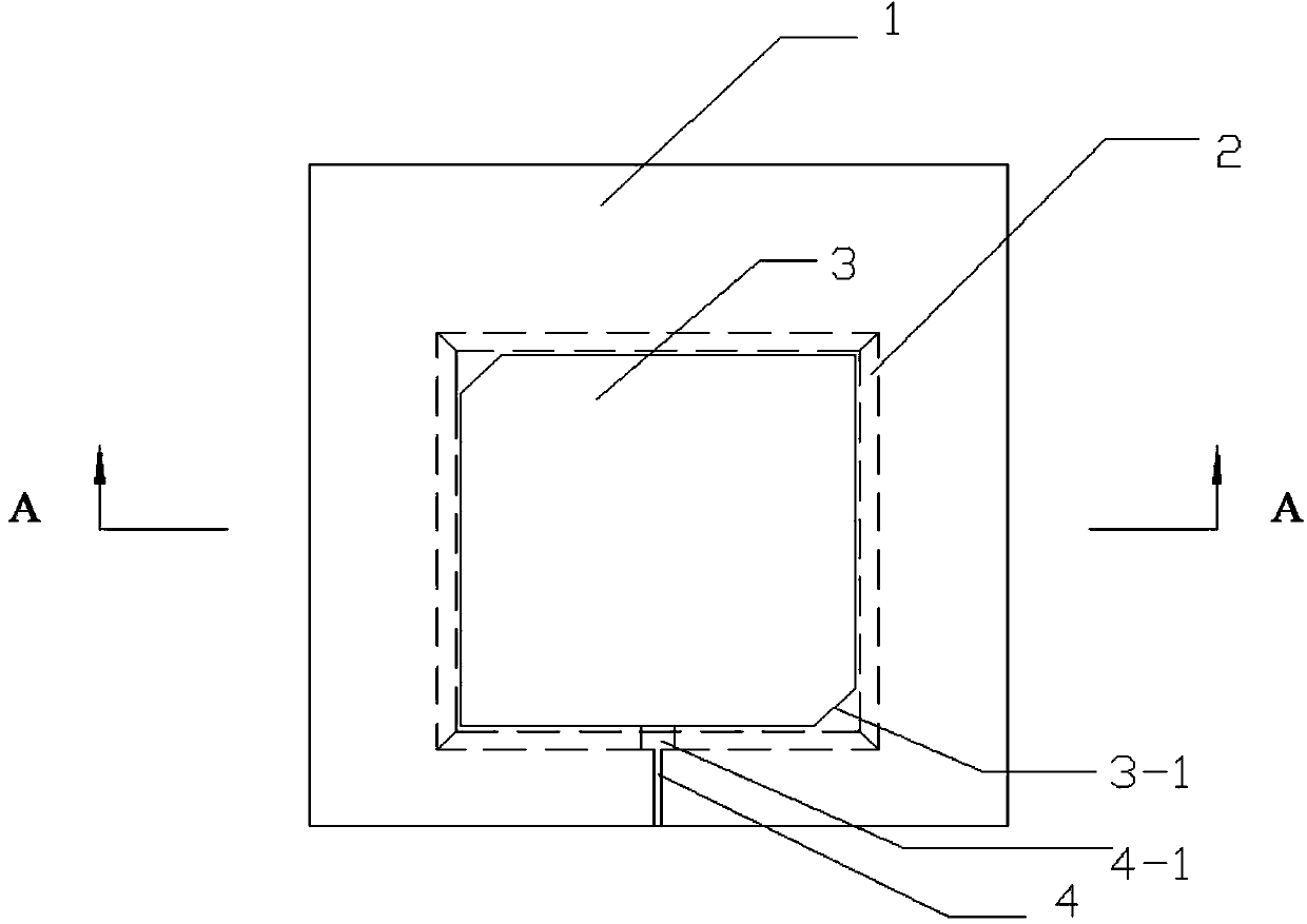
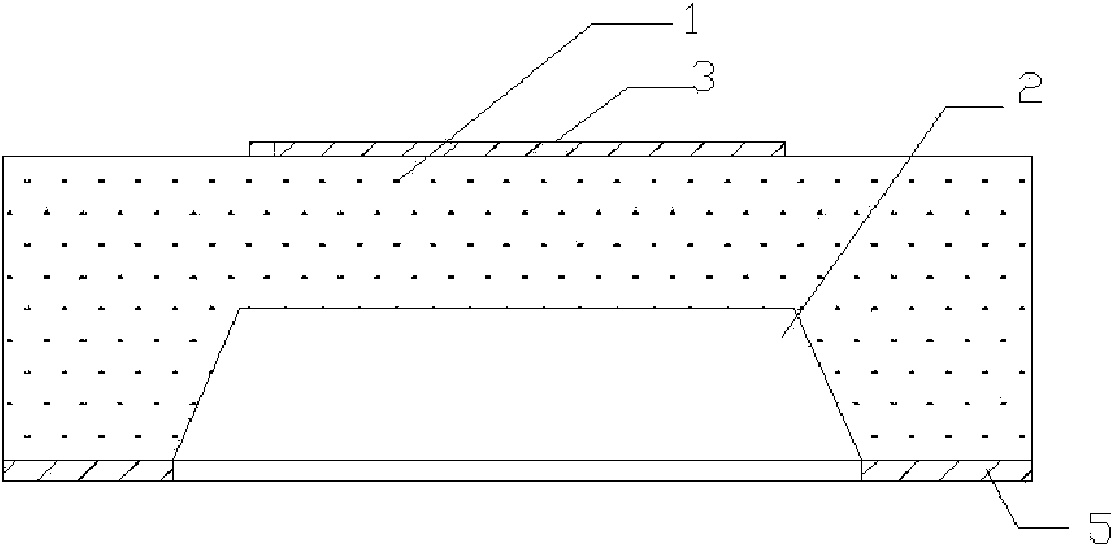
[0017] In this embodiment, the single-patch microstrip antenna is taken as an example: the relative permittivity of the high-resistance silicon substrate 1 is 11.9, the resistivity is 20000Ω·cm, the loss tangent is 0.005, the crystal orientation is [111], and the volume (length×width×thickness ) 11.2mm×11.2mm×300μm, the conical angle of the truncated pyramid groove 2 is 45°, the upper surface of the groove (length×width) 6.426×6.426mm, the lower mouth (length×width) 6.726×6.726mm , the depth of the groove is 150 μm; the radiation patch 3 (length×width) is 6.20×6.20mm, and the length of the degenerate separation unit 3-1 on it is 0.9899mm (the length is cut from the lower right corner and the upper left corner of the radiation patch 3 respectively. Take the isosceles triangle whose length is 0.7mm on both sides), feeder impedance 50Ω, feeder: 4 (length × width) 2.5 × 0.072mm, 4-1 (length × width) 0.290 × 0.280mm; grounding piece 5 (length x width) 11.2 x 11.2mm, a square hole (...

Embodiment 2

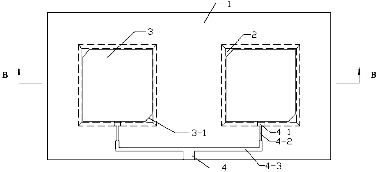
[0020] The present invention takes a binary antenna device with a working frequency of 12 GHz as an example: the high-resistance silicon substrate 1 adopts high-resistance silicon with a resistivity of 20,000 Ω cm, a relative permittivity of 11.9, a loss tangent of 0.005, and a crystal orientation of [100]. , the base (length × width × thickness) 21.0mm × 15.4mm × 500μm, the bottom of the regular quadrangular pyramid truncated groove 2 symmetrically set two upper bottom surfaces (length × width) 6.426 × 6.426mm, the lower bottom mouth (length × width) 6.780×6.780mm, truncated square groove with a groove depth of 250μm; each radiation patch 3 (length×width) 6.20×6.20mm, and the length of each degenerate unit 3-1 on it is 0.9899mm (the length is between two The lower right corner and the upper left corner of the radiation patch 3 are obtained by cutting off an isosceles triangle whose sides are both 0.7mm in length); the impedance of the connecting section between the feeder and ...


PUM


Abstract

The invention belongs to the technical field of antennas, and provides a high-frequency micro-strip antenna with a substrate made of high resistance silicon. The high-frequency micro-strip antenna comprises the substrate made of high resistance silicon, right-square-pyramid-frustum-shaped grooves, radiation patches, feeder lines of the radiation patches and a ground lug, wherein the right-square-pyramid-frustum-shaped grooves are formed in the bottom of the substrate, and the radiation patches are arranged on the upper surface of the substrate and provided with degeneration units. Due to the fact that air slots in the reverse side of the substrate made of high resistance silicon are designed into the right-square-pyramid-frustum-shaped grooves, MEMS wet etching can be adopted, the conical surfaces of the right-square-pyramid-frustum-shaped grooves are automatically etched into conical surfaces of which the angle is the same as the material crystal orientation interfacial angle, a waste masking layer cannot be generated, and the etching speed and flatness of the top surfaces of the grooves are respectively increased by about 10 times and 20 times of the etching speed and flatness in the background technology. The high-frequency micro-strip antenna has the advantages that the structural design of the antenna is advanced, the production process is easy and convenient to conduct, production efficiency is high, the yield is high, microwave losses are low, radiation efficiency is high, the performance of the antenna is excellent, the antenna is easily integrated to form an array type micro-strip antenna, production cost is low, and the requirements for large-scale production can be met.

Description

technical field [0001] The invention belongs to the technical field of microstrip antennas, in particular to an X-band microstrip antenna using high-resistance silicon as a base and having a truncated pyramid-shaped air slot on the back of the base; the antenna has high efficiency, high gain, high power, and It is easy to integrate to form an array microstrip antenna, which can be widely used in technical fields such as fishing boat navigation, deep space communication, and intelligent transformation of conventional ammunition. Background technique [0002] At present, in conventional deep space communication, civilian fishing boat navigation, ammunition intelligent transformation, unmanned aerial vehicle communication, etc., there are high requirements for light equipment, that is, small size, light weight, low power consumption, and digital technology. From the introduction of the concept of microstrip antennas in the 1950s, to the development and manufacture of practical ...

Claims


Application Information

Patent Timeline
Patent Type & Authority Applications(China)
IPC IPC(8): H01Q1/38H01Q1/48H01Q21/00H01Q13/08
Inventor 刘晓明陈焕晖黎业飞郝晓红谢晓梅洪泉邓振雷朱钟淦
Owner UNIV OF ELECTRONICS SCI & TECH OF CHINA
Why Eureka
Try Eureka