Front electrode diffraction type local back surface field passivation type crystalline silicon cell preparation method

A technology of crystalline silicon battery and localized back field, which is applied in the direction of circuits, electrical components, semiconductor devices, etc., to achieve the effect of improving the utilization rate

Active Publication Date: 2014-04-23
HUNAN RED SUN PHOTOELECTRICITY SCI & TECH
View PDF8 Cites 10 Cited by
  • Summary
  • Abstract
  • Description
  • Claims
  • Application Information

AI Technical Summary

Problems solved by technology

[0005] The advantages of high processing precision and strong stability of the laser can meet the needs of the photovoltaic industry. The front electrode diffraction technology

Method used


Image

  • Front electrode diffraction type local back surface field passivation type crystalline silicon cell preparation method
  • Front electrode diffraction type local back surface field passivation type crystalline silicon cell preparation method
  • Front electrode diffraction type local back surface field passivation type crystalline silicon cell preparation method

Examples


Embodiment 1

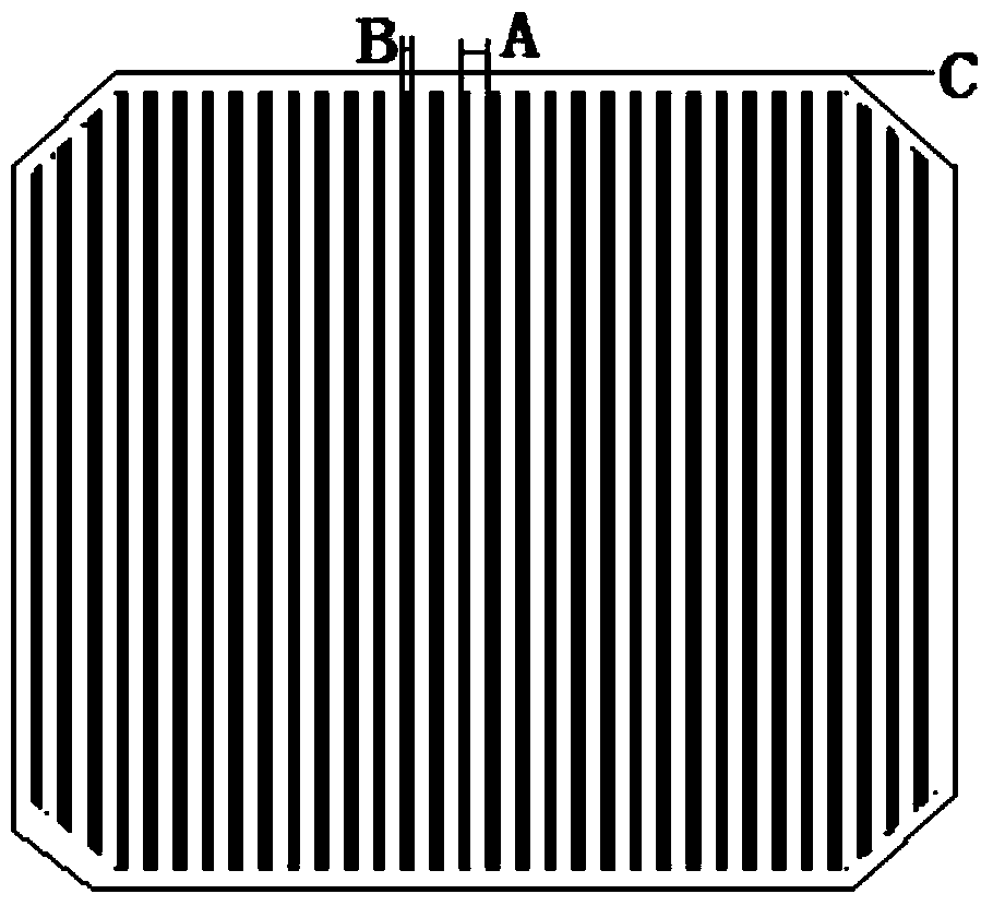
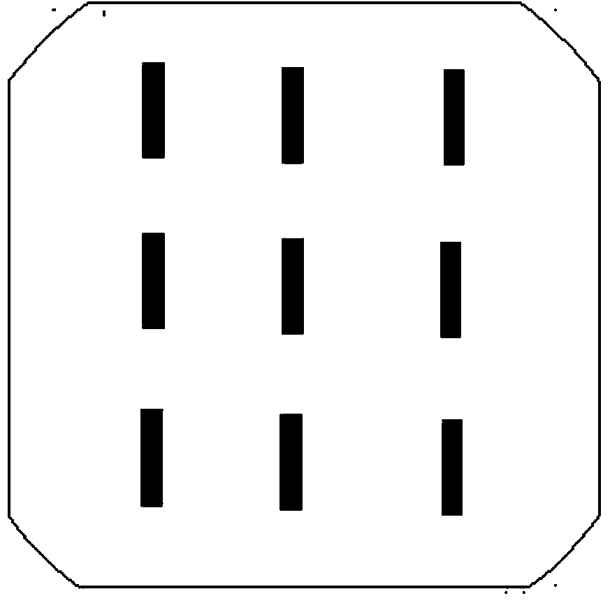
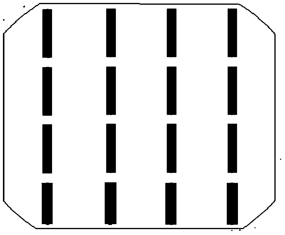
[0036] see Figure 1 to Figure 5 , the preparation method of the front electrode diffraction type localized back field passivation crystalline silicon cell comprises the following steps in turn:

[0037] (1) Choose 156×156mm with a resistivity of 1~3Ω·cm 2 P-type monocrystalline silicon wafer is used as the substrate. To balance the impact of series resistance and shading area on battery performance, a nanosecond green laser with a wavelength of 532nm is used to open 4 rows of holes from the back surface of the silicon wafer. The diameter of the holes is 1.5-2.2mm. The spacing of each row of holes is 12-20mm; the hole array see figure 1 4 rows of small holes in the middle;

[0038] (2) Texture the silicon wafer by single crystal wet method, and prepare a P-N junction with a sheet resistance value of 85-95Ω / □ on the silicon wafer by high-temperature diffusion; the high-temperature diffusion adopts a conventional diffusion furnace, and the parameter settings are shown in Table ...


PUM

PropertyMeasurementUnit
Resistanceaaaaaaaaaa
Wavelengthaaaaaaaaaa

Abstract

The invention discloses a front electrode diffraction type local back surface field passivation type crystalline silicon cell preparation method. A row of cavities which are arranged uniformly are formed in a silicon wafer substrate at the front electrode main gate position through a laser device to replace the main gate electrode and the gate electrode is led to the back surface of the cell to reduce the shading area of the main gate electrode and place the front electrode on the back surface; a layer of Al2O3 is deposited on the back surface of the silicon wafer through atomic layer deposition or the PECVD method to passivate the back surface f the cell, a layer of thick SiNx is deposited on the surface of the film to protect the passivation effect of the Al2O3, and then a back open-membrance pattern is designed, and a back electrode conductive window is prepared through laser or chemical corrosion method; and the back electrode, a back matched aluminum back surface field, a back front electrode and a front gate electrode are printed successively, and the printing and sintering processes are optimized to make the electrode contact region has the advantage of good filling effect.

Description

technical field [0001] The invention belongs to the field of preparation of crystalline silicon batteries, and in particular relates to a preparation method of a front electrode diffraction type local back field passivation crystalline silicon battery. Background technique [0002] It has become a general consensus in the domestic industry to promote the steady and sustainable development of the photovoltaic industry by accelerating industrial restructuring and technological progress. According to the "Several Opinions on Promoting the Healthy Development of the Photovoltaic Industry" issued at this stage, the state will give priority to supporting photovoltaic projects with monocrystalline silicon cell efficiency above 20% and polycrystalline silicon cell efficiency above 18%. To meet this requirement, the use of new technologies and new tools to prepare high-efficiency structural batteries has become the main way for the industry to improve its competitiveness. [0003] T...

Claims


Application Information

Patent Timeline
IPC IPC(8): H01L31/18H01L31/0224
CPCH01L31/02167H01L31/02245H01L31/1804Y02P70/50
Inventor 姬常晓周子游刘文峰
Owner HUNAN RED SUN PHOTOELECTRICITY SCI & TECH
Why Eureka
Try Eureka