
Method for preparing superlattice nanowire array assembled by tellurium-lead telluride nanocrystals

A nanowire array and lead telluride technology, applied in chemical instruments and methods, nanotechnology, single crystal growth, etc., to achieve composition and structure control, simple preparation method, and great application prospects

Inactive Publication Date: 2014-04-30
DALIAN UNIV OF TECH
View PDF0 Cites 10 Cited by
  • Summary
  • Abstract
  • Description
  • Claims
  • Application Information

AI Technical Summary

Problems solved by technology

However, compared to the extensive research on superlattices of various heterogeneous materials, the preparation method of superlattice nanowires assembled by Te-PbTe nanocrystals has not been reported publicly.

Method used

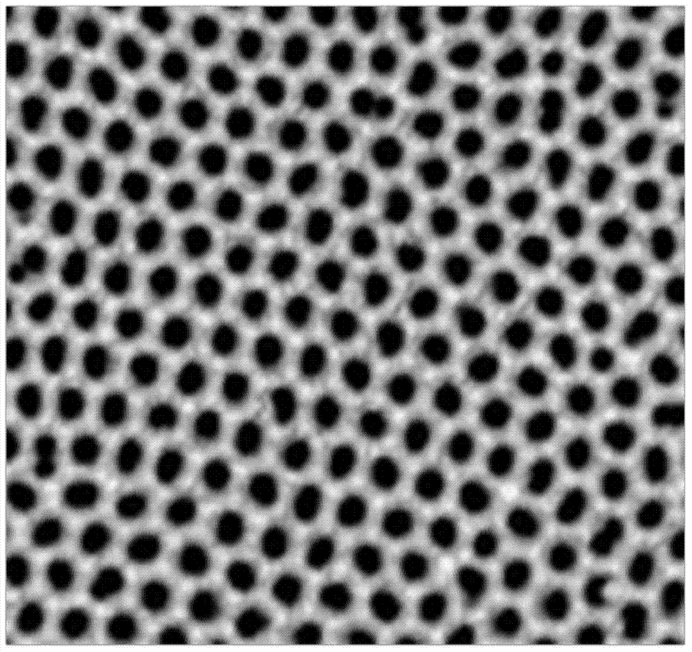
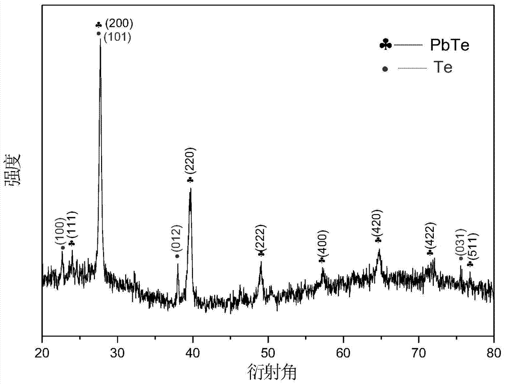
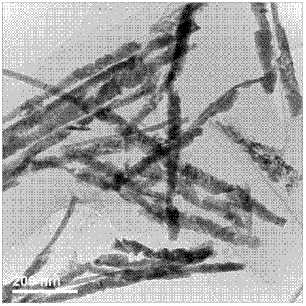

Image

  • Method for preparing superlattice nanowire array assembled by tellurium-lead telluride nanocrystals
  • Method for preparing superlattice nanowire array assembled by tellurium-lead telluride nanocrystals
  • Method for preparing superlattice nanowire array assembled by tellurium-lead telluride nanocrystals

Examples


Embodiment 1

[0021] A PAA template is prepared by a secondary anodic oxidation method, and a 100nm-200nm gold film is sputtered and evaporated on its back as an electrode. Then prepare the electrodeposition solution, the solution is made of TeO 2 , Pb(NO 3 ) 2 , tartaric acid, ethanol, HNO 3 Solution composition. Dissolve 3g of tartaric acid in a small amount of deionized water first, then add 5mM TeO 2 , under the condition of constant temperature magnetic stirring at 60℃, add HNO dropwise with a dropper 3 When the solution was clear, add 5mMPb (NO 3 ) 2 , continue to drop HNO with dropper 3 The solution became clear. Add 20ml of ethanol and deionized water to make a 100ml solution, and stir evenly. by dropwise addition of HNO 3 Make the solution pH 1. Using a pulsed electrochemical deposition method, a gold-sprayed PAA template was used as the anode and graphite as the cathode. Before the electrodeposition, in order to make the solution contact with the surface of the PAA tem...

Embodiment 2

[0026] A PAA template is prepared by a secondary anodic oxidation method, and a 100nm-200nm gold film is sputtered and evaporated on its back as an electrode. Then prepare the electrodeposition solution, the solution is made of TeO 2, Pb(NO 3 ) 2 , tartaric acid, ethanol, HNO 3 Solution composition. Dissolve 3g of tartaric acid in a small amount of deionized water first, then add 5mM TeO 2 , under the condition of constant temperature magnetic stirring at 60℃, add HNO dropwise with a dropper 3 When the solution was clear, add 5mMPb (NO 3 ) 2 , continue to drop HNO with dropper 3 The solution became clear. Add 20ml of ethanol and deionized water to prepare a 100ml solution, and stir evenly. by dropwise addition of HNO 3 Make the solution pH 1. Using a pulsed electrochemical deposition method, a gold-sprayed PAA template was used as the anode and graphite as the cathode. Before the electrodeposition, in order to make the solution contact with the surface of the PAA t...


PUM

PropertyMeasurementUnit
pore sizeaaaaaaaaaa
diameteraaaaaaaaaa

Abstract

The invention relates to a method for preparing superlattice nanowire array assembled by tellurium-lead telluride nanocrystals and belongs to the technical field of nanometer material preparation. The method is characterized by comprising the following steps: selecting porous anodized alumina (PAA) prepared by utilizing a two-step anodization method as a template; applying a negative bias voltage in electrolyte containing Pb and Te ions by virtue of a pulse electrochemical deposition technique, and alternatively carrying out electrochemical deposition of PbTe and Te elements in pore paths of the PAA, so as to finally obtain the superlattice nanowire array assembled by Te-PbTe nanocrystals. The method has the effects and the advantages that a product is an orderly-arranged superlattice nanowire array which is assembled by the tellurium-lead telluride nanocrystals and is alternatively formed by two different materials, namely tellurium nanocrystals and lead telluride nanocrystals; the preparation method is simple, the cost is low, and the components and structure of the array are easy to adjust and control; the superlattice nanowire array has important potential application prospects in the fields of energy sources, thermoelectricity, optics, electrics and the like.

Description

technical field [0001] The invention belongs to the technical field of nanometer material preparation, and relates to a method for preparing a tellurium-lead telluride (Te-PbTe) crystal assembled superlattice nanowire array. Background technique [0002] With the development of nanotechnology, people have been able to prepare various low-dimensional mesoscopic structures such as quantum wires, quantum wells, and superlattices. In these mesoscopic structures, because the coherence length of the electron wave function is equivalent to the characteristic length of the system, the physical properties of the electron are completely governed by the laws of quantum mechanics, and the wave nature of the electron is fully reflected in the transport process. A semiconductor superlattice is a multi-layer heterostructure crystal grown alternately from two different materials in a few nanometers to tens of nanometers. Due to the different band gaps of the two materials, potential wells ...

Claims


Application Information

Patent Timeline
Patent Type & Authority Applications(China)
IPC IPC(8): C30B7/12C30B29/62C30B29/68C30B29/46B82Y40/00
Inventor 薛方红汪晓允黄昊刘璐董星龙
Owner DALIAN UNIV OF TECH
Learn More