
Semiconductor device and forming method thereof

A semiconductor and device technology, applied in the field of semiconductor devices and their formation, can solve problems such as poor performance, and achieve the effect of saving process time and simplifying process steps

Active Publication Date: 2014-05-07
SEMICON MFG INT (SHANGHAI) CORP
View PDF3 Cites 2 Cited by
  • Summary
  • Abstract
  • Description
  • Claims
  • Application Information

AI Technical Summary

Problems solved by technology

[0006] However, in the prior art, the common gate electrode CMOS transistor with high K gate dielectric layer and metal gate electrode has poor performance

Method used


Image

  • Semiconductor device and forming method thereof
  • Semiconductor device and forming method thereof
  • Semiconductor device and forming method thereof

Examples


no. 1 example

[0032] Figure 6 to Figure 11 It is a schematic cross-sectional structure diagram of the formation process of the semiconductor device described in the first embodiment of the present invention.

[0033] Please refer to Image 6 , provide a semiconductor substrate 300, the semiconductor substrate 300 includes adjacent first region I and second region II; form a dummy gate layer 301 on the surface of the semiconductor substrate 300, and cover the dummy gate layer The first dielectric layer 302 on the sidewall of 301, the dummy gate layer 301 is located on the surface of the semiconductor substrate 300 in the first region I and the second region II, and the surface of the first dielectric layer 302 and the dummy The surface of the gate layer 301 is flush.

[0034] The semiconductor substrate 300 is used to provide a working platform for subsequent processes; the semiconductor substrate 300 is a silicon substrate, a silicon-germanium substrate, a silicon carbide substrate, a si...

no. 2 example

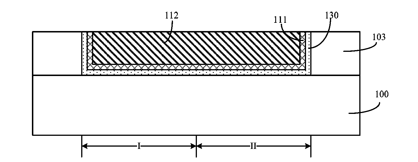
[0073] Figure 12 to Figure 14 It is a schematic cross-sectional structure diagram of the formation process of the semiconductor device described in the second embodiment of the present invention.

[0074] Please refer to Figure 12, provide a semiconductor substrate 200, the semiconductor substrate 200 includes adjacent first region I and second region II; form a dummy gate layer (not shown) on the surface of the semiconductor substrate 200, and cover the The first dielectric layer 202 on the sidewall of the dummy gate layer, the dummy gate layer is located on the surface of the semiconductor substrate 200 in the first region I and the second region II, the surface of the first dielectric layer 202 is in contact with the The surface of the dummy gate layer is flush; the dummy gate layer is removed until the semiconductor substrate 200 is exposed, forming a first opening; forming in the first opening: covering the sidewall and bottom of the first opening The high K dielectri...


PUM


Abstract

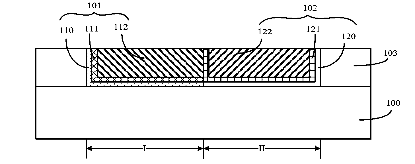
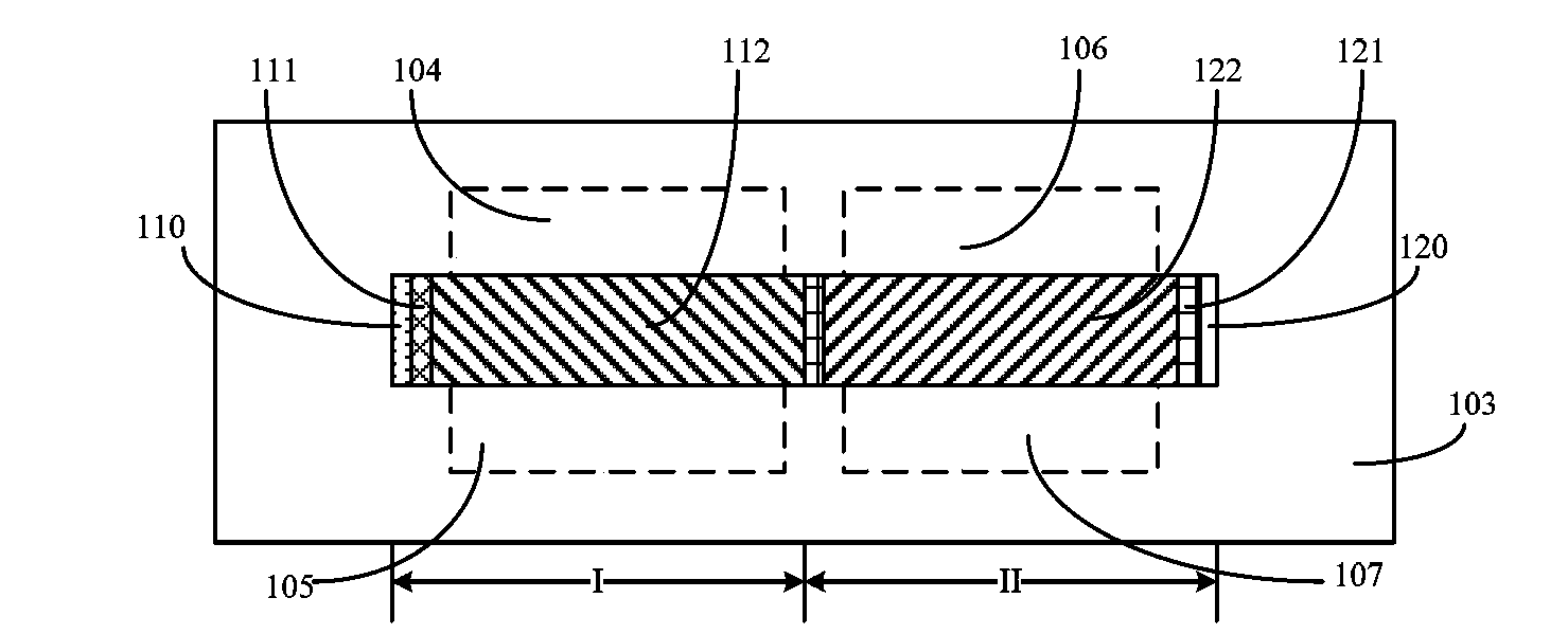
The invention discloses a semiconductor device and a forming method thereof. The semiconductor device comprises a semiconductor substrate, a first gate structure, a second gate structure, a second dielectric layer and a first conductive plug, wherein the semiconductor substrate comprises a first region and a second region near to each other; the first gate structure is located on the surface of the semiconductor substrate in the first region, and the first gate structure comprises a first high K gate dielectric layer, a first work function layer located on the surface of the first high K gate dielectric layer and a first gate electrode layer located on the surface of the first work function layer; the second gate structure is located on the surface of the semiconductor substrate in the second region, and the second gate structure comprises a second high K gate dielectric layer, a second work function layer located on the surface of the second high K gate dielectric layer and a second gate electrode layer located on the surface of the second work function layer; the second dielectric layer is located on the surface of the first gate structure and the second gate structure, and the second dielectric layer is internally provided with a contact through hole exposed out of part of the first gate structure and part of the second gate structure; and the first conductive plug is formed and located in the contact through hole. Performances of the semiconductor device are good.

Description

technical field [0001] The invention relates to the technical field of semiconductor manufacturing, in particular to a semiconductor device and a forming method thereof. Background technique [0002] Complementary Metal-Oxide-Semiconductor (CMOS) has become a commonly used semiconductor device in integrated circuits. The CMOS transistors include: P-type metal oxide semiconductor transistors (PMOS) and N-type metal oxide semiconductor transistors (NMOS). In the prior art, in order to control the short channel effect while reducing the gate size, high-K dielectric materials are used to replace conventional silicon oxide and other materials to form gate dielectric layers, and metal materials are used to replace conventional polysilicon and other materials to form gate electrode layers; in addition , in order to adjust the threshold voltage of the PMOS tube and the NMOS tube, the existing technology will form a work function layer (work function layer) on the surface of the gat...

Claims


Application Information

Patent Timeline
Patent Type & Authority Applications(China)
IPC IPC(8): H01L21/28H01L21/8238H01L29/423H01L27/092
CPCH01L21/823437H01L21/82345H01L21/823475H01L27/092
Inventor 洪中山
Owner SEMICON MFG INT (SHANGHAI) CORP
Learn More