Jacket-layer sliding type friction nanometer generator
A technology of nano generators and generators, applied in the direction of friction generators, etc., can solve the problems of power supply components that cannot be used for microelectronic devices, complex structures, and large volumes of generators, and achieve convenient packaging technology, extended application range, and energy efficiency. The effect of efficient use
- Summary
- Abstract
- Description
- Claims
- Application Information
AI Technical Summary
Problems solved by technology
Method used
Image
Examples
Embodiment 1
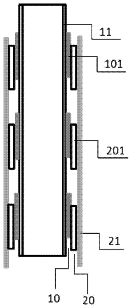
[0116] The first conductive element is a metal copper sheet with a size of 6.4cm×3.8cm, the second conductive element is a metal aluminum sheet with a size of 6.4cm×4.5cm, and the material of the first friction unit is Teflon (polytetrafluoroethylene) film. The material of the second friction unit is polyethylene terephthalate (PET). Polytetrafluoroethylene and polyethylene terephthalate have extremely negative and extremely positive polarities, respectively, in the triboelectric series. Teflon is made into two strip film structures with length, width and height of 6cm, 1.6cm and 0.2cm respectively, and according to Image 6 In the same way, the conductive glue is pasted on the copper sheet at intervals, and the polyethylene terephthalate is distributed on the aluminum sheet with the same size and interval. Roll the copper sheet pasted with Teflon into a cylinder around a plastic rod with a diameter of about 0.6cm and a length of 10cm and fix the two ends with adhesive strips...
Embodiment 2
[0119] This embodiment is basically the same as Embodiment 1, the only difference is that: a silicon wafer with a thickness of 600 μm is used as the second friction unit material, and a layer of photoresist is coated on the surface of the silicon wafer by rotation A square window array with a side length of micron or sub-micron level is formed on the glue, and the silicon wafer after photolithography is chemically etched with hot potassium hydroxide to form a pyramid-shaped concave structure array at the window. Then divide it into small pieces with a length of 2 cm and a width of 2 cm, and arrange them on the surface of the second conductive element in a checkerboard shape; The pattern of the same checkerboard-shaped Ag thin layer, the thin layer also serves as the first conductive element. When the silicon chip and the two materials of Ag are in contact with each other under the action of external force and relatively slide, because the surface of the silicon chip has a conc...
Embodiment 3
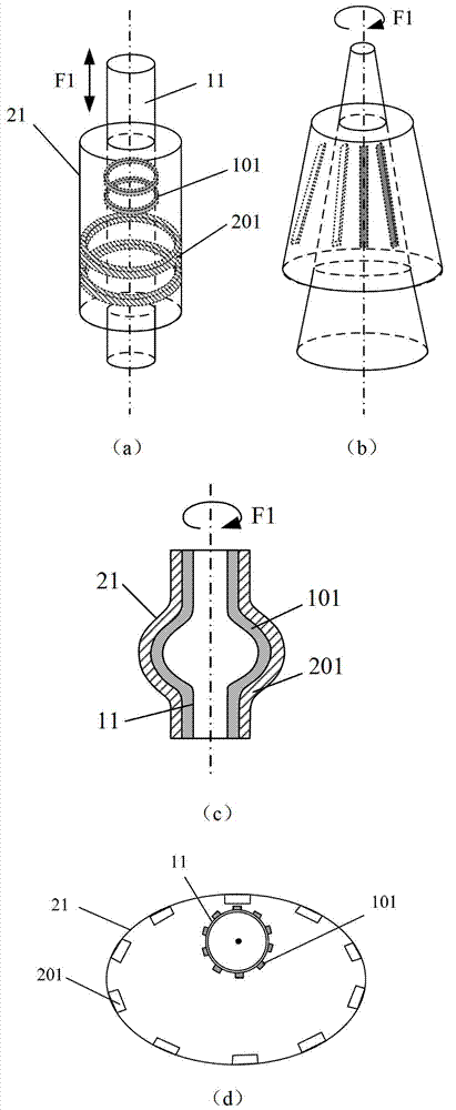
[0121] This embodiment is basically the same as Embodiment 1, the difference is that firstly through conventional methods such as mask-etching-metal deposition-mask removal, a hexagonal polychloride sleeve is formed such as Figure 5 For the annular gold Au strip shown, the width of the strip along the axial direction is about 100 μm. Then continue to prepare polydimethylsiloxane (PDMS) ring strips on the top of the gold strips by spin coating and etching as the first friction unit, and further prepare nanowire arrays on the surface by inductively coupled plasma etching , the specific steps are: deposit about 10 nanometers of gold on the surface of PDMS with a sputtering device, then put the PDMS film into an inductively coupled plasma etching machine, etch the side where the gold is deposited, and pass through O 2 , Ar and CF 4 Gas, the flow rate is controlled at 10sccm, 15sccm and 30sccm respectively, the pressure is controlled at 15mTorr, the working temperature is control...
PUM
 Abstract
Description
Claims
Application Information


