
Small pulsed electric field and magnetic field integrated measurement device

A pulsed electric field and small pulse technology, applied in the direction of electromagnetic field characteristics, etc., can solve the problems of inability to obtain pulsed electric field and pulsed magnetic field, consume a lot of manpower and material resources, inconvenience, etc., achieve low cost, improve the ability and speed of anti-electromagnetic interference quick effect

Active Publication Date: 2014-05-28
PLA UNIV OF SCI & TECH
View PDF4 Cites 9 Cited by
  • Summary
  • Abstract
  • Description
  • Claims
  • Application Information

AI Technical Summary

Problems solved by technology

Regardless of whether it is cable transmission or optical fiber transmission, it is inconvenient in multi-point distributed measurement. Multiple digital acquisition and storage devices are required, as well as a large number of cables, and the acquisition and storage devices must be placed in an electromagnetic shielding room or a shielding cabinet to prevent pulses. Electromagnetic fields interfere with it
Moreover, the traditional pulsed electric field and pulsed magnetic field measurement sensors are separated, and the two physical quantities cannot be integrated and synchronized at the same point, and the relationship between the pulsed electric field and the pulsed magnetic field at the same time cannot be obtained.
In a large-scale pulse electromagnetic environment measurement, traditional measurement methods often consume a lot of manpower and material resources

Method used


Image

  • Small pulsed electric field and magnetic field integrated measurement device
  • Small pulsed electric field and magnetic field integrated measurement device
  • Small pulsed electric field and magnetic field integrated measurement device

Examples


Embodiment Construction

[0027] Embodiments of the present invention will be described in detail below in conjunction with the accompanying drawings.

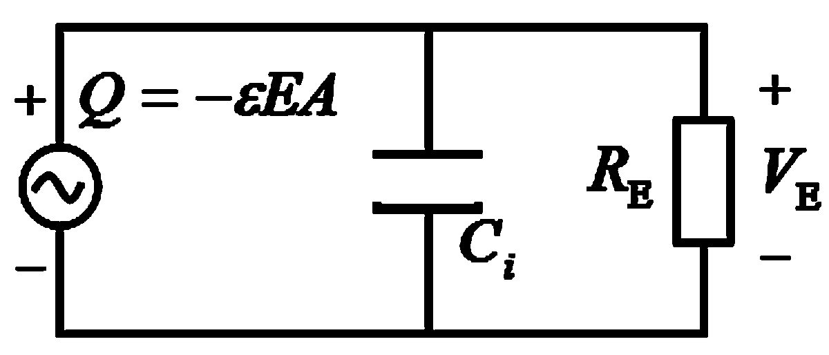
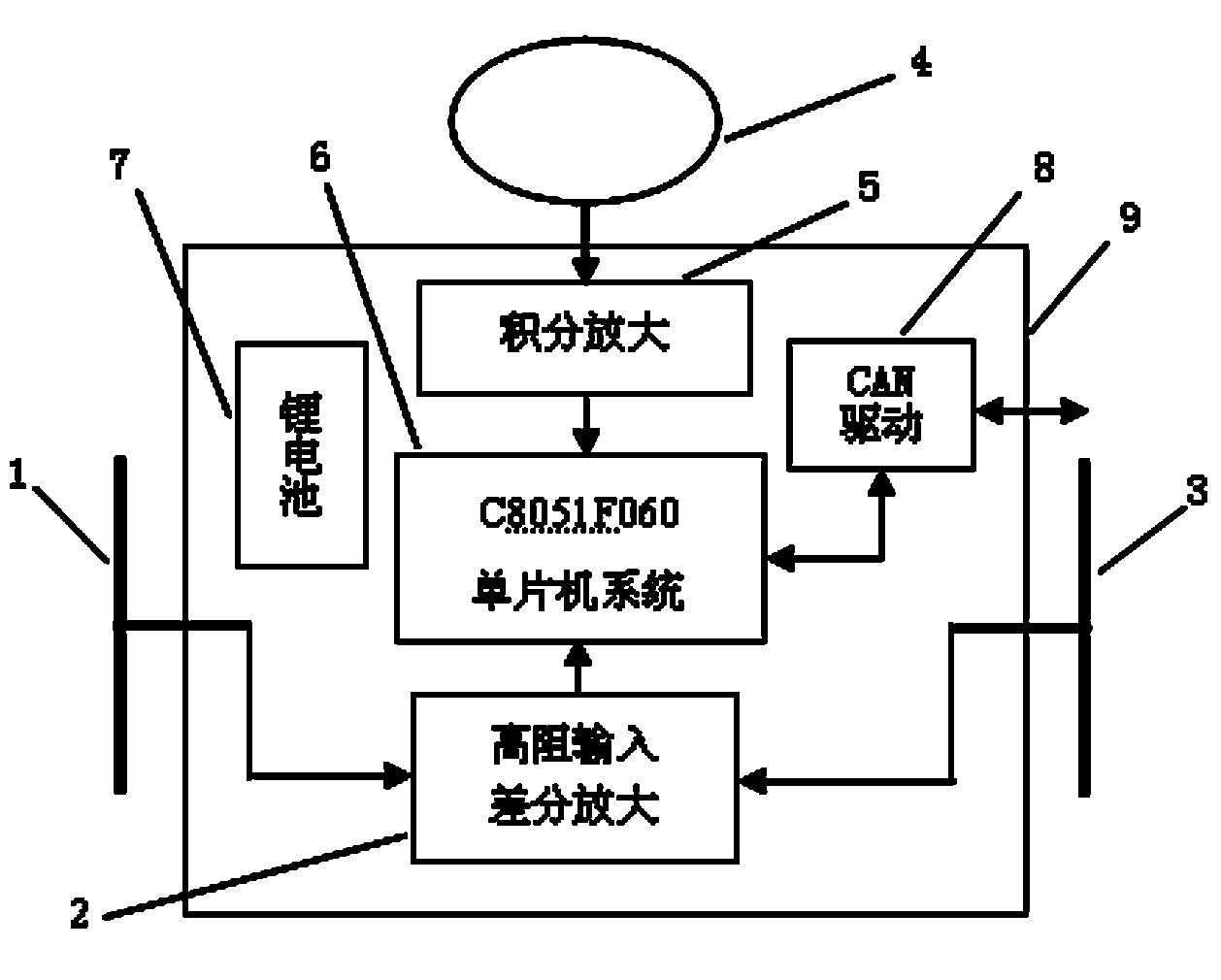
[0028] Such as figure 1 As shown, the circular flat panel electric field antenna 1 and the circular flat panel electric field antenna 3 form a pair of electric field sensors with a differential structure, which are installed on two opposite sides of the hexahedral metal shielding shell 9, and convert the electric field signal into a differential voltage signal, The differential amplifier circuit 2 that is input to the high-impedance input in the metal shielding shell 9 through the metal rod, the output of the differential amplifier circuit 2 is connected to the input end of the 16-bit high-speed analog-to-digital conversion ADC0 of the C8051F060 single-chip microcomputer 6 .

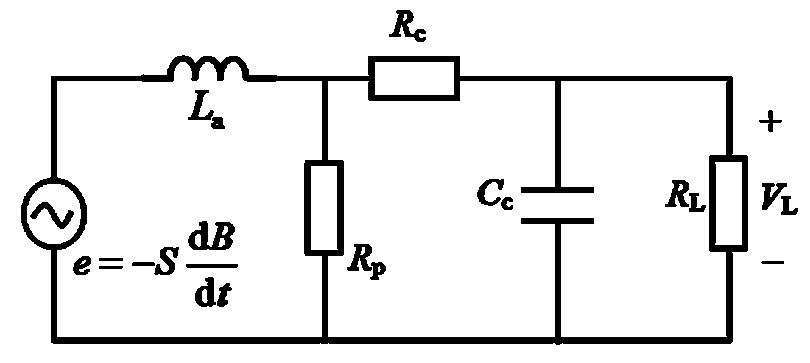
[0029] Such as figure 1 As shown, a small loop magnetic field antenna 4 is installed on the top surface of the hexahedral metal shielding shell 9 . The small-ring magnetic fie...


PUM


Abstract

The invention discloses a small pulsed electric field and magnetic field integrated measurement device. The small pulsed electric field and magnetic field integrated measurement device comprises a high-performance composite signal processing single-chip microcomputer collecting system, an electric field antenna, a high-resistance differential amplification circuit, a small loop magnetic field antenna, an integral circuit and a hexahedron metal shielding shell. Electric field signals are collected by an ADC0 module of a single-chip microcomputer. Magnetic field signals are collected by an ADC1 module of the single-chip microcomputer. All the circuits are packaged in the hexahedron metal shielding shell. An ADC0GT register and an ADC0LT register of a single-chip microcomputer chip are installed to start the window detection function of an analog-digital conversion module ADC0 to achieve pretrigger, and random overall pulse waveforms are collected by combining DMA circulating storage data. Data exchange is carried out between a collecting system and the outside through a CAN high-speed transmission interface. At the same measurement point, pulsed electric field waveforms and pulsed magnetic field waveforms can be measured at the same time in the measurement process at one time. The device is low in cost, high in work efficiency and strong in anti-jamming capability.

Description

technical field [0001] The invention relates to a small pulse electric field and magnetic field measuring device, in particular to an integrated digital measuring device for synchronously measuring pulse electric field and pulse magnetic field in a transient pulse electromagnetic field interference environment. Background technique [0002] Transient electromagnetic pulse interference exists in many environments, such as the switching action of electrical appliances in factories, the action of power electronic devices in substations, and the lightning discharge process in nature. In order to assess these pulse electromagnetic interference hazards, they need to be measured to obtain their time-domain characteristics and frequency-domain characteristics, such as pulse peak value, pulse rise time, pulse half-height width, and spectral distribution. In addition, the measurement of electromagnetic pulses in small spaces in complex large systems is an important aspect that plagues...

Claims


Application Information

Patent Timeline
Patent Type & Authority Applications(China)
IPC IPC(8): G01R29/08
Inventor 李炎新石立华江志东高成苏丽媛陆峰郭飞邱实
Owner PLA UNIV OF SCI & TECH
Learn More