Silicon nitride manufacturing method

A manufacturing method and technology of silicon nitride, which are applied in semiconductor/solid-state device manufacturing, gaseous chemical plating, coating, etc., can solve the problem of the difficulty of integrating double strained lining layers with tensile stress silicon nitride, etc., and achieve enhanced Si- Effects of N-bonding force, increased film density, improved performance and reliability

Inactive Publication Date: 2014-06-04
INST OF MICROELECTRONICS CHINESE ACAD OF SCI
View PDF4 Cites 16 Cited by
  • Summary
  • Abstract
  • Description
  • Claims
  • Application Information

AI Technical Summary

Problems solved by technology

[0008] It can be seen that under the same etching conditions, the etch rate of tensile stress silicon nitride in dHF is significantly higher than that of compressive stress silicon nitride and thermal oxide, making it difficult to integrate tensile stress in the double strained liner of the gate-last process. Silicon nitride

Method used


Image

  • Silicon nitride manufacturing method
  • Silicon nitride manufacturing method
  • Silicon nitride manufacturing method

Examples


Embodiment Construction

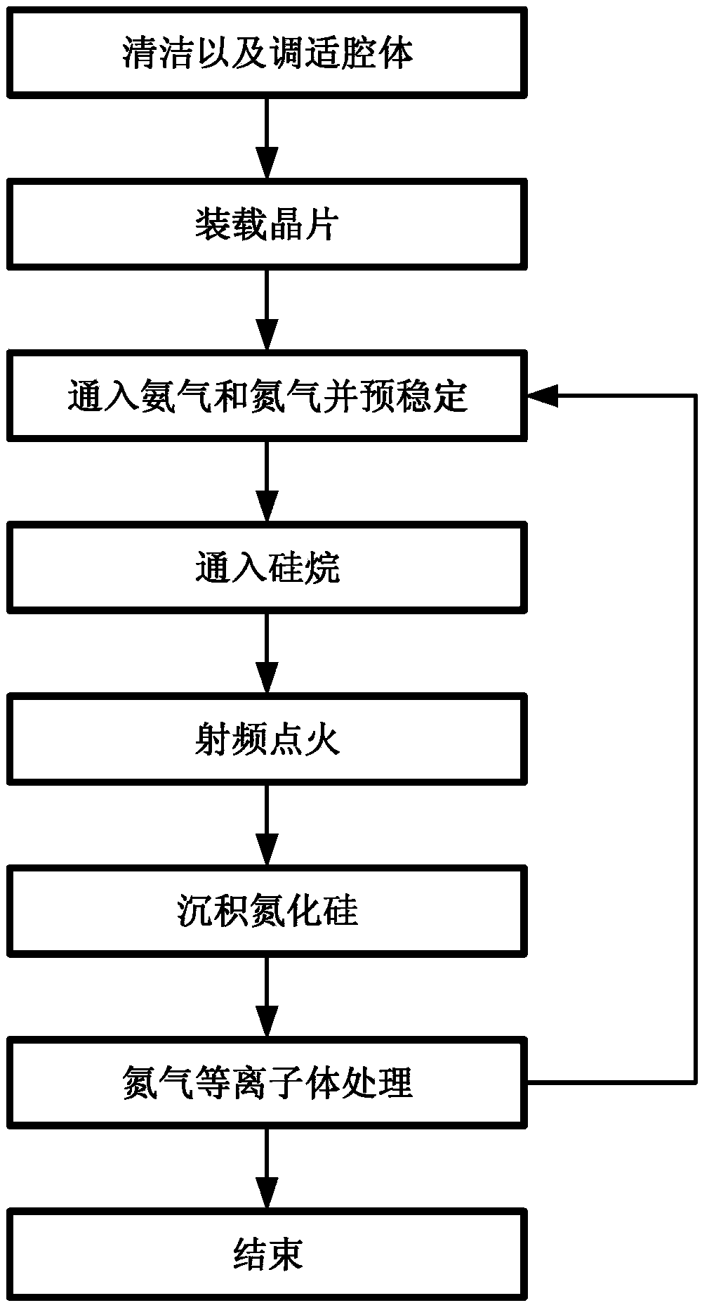
[0030] The features and technical effects of the technical solution of the present invention will be described in detail below with reference to the accompanying drawings and in combination with schematic embodiments, and a manufacturing method capable of effectively enhancing the density and stress of tensile-stressed silicon nitride films is disclosed. It should be pointed out that similar reference numerals represent similar structures, and the terms "first", "second", "upper", "lower" and the like used in this application can be used to modify various device structures or process steps . These modifications do not imply spatial, sequential or hierarchical relationships of the modified device structures or process steps unless otherwise specified.

[0031] In one embodiment of the present invention, the method for depositing the tensile stress silicon nitride film is PECVD process, and the equipment used is dual-frequency capacitively coupled plasma parallel-plate PECVD equ...


PUM


Abstract

The invention discloses a silicon nitride manufacturing method. The method comprises the following steps: step c1, carrying out introduction of ammonia gas and nitrogen and carrying out pre-stabilization processing; step c2, carrying out silane introduction; step c3, carrying out radio frequency ignition; step c4, carrying out silicon nitride deposition; and step c5, using nitrogen plasma to carry out processing on the silicon nitride. According to the manufacturing method, nitrogen plasma bombardment is used for strengthening the Si-N binding force, thereby enhancing the film density. The acidoresistance of the silicon nitride with the tensile stress is improved, so that the silicon nitride with the tensile stress can be applied to the dual-stress lining layer rear grid process. And thus the performance and reliability of the device are effectively enhanced.

Description

technical field [0001] The invention relates to a semiconductor device manufacturing method, in particular to a strained silicon nitride manufacturing method with tensile stress. Background technique [0002] When the physical gate length of the device continues to shrink, if an attempt is made to maintain good performance of the device, the carrier mobility enhancement technology is crucial for the scaling down of CMOS. [0003] Strained silicon technology improves the switching speed of devices by only enhancing the carrier mobility, which has become a hot research topic. [0004] Recently, coaxial process strained silicon has been widely used in high performance logic technology. Enhanced NMOS carrier mobility has been developed by introducing channel strain through a tensile-stressed nitride capping layer on the device structure. Likewise, a compressively stressed nitride capping layer can be formed on the device structure to enhance PMOS carrier mobility. Using the a...

Claims


Application Information

Patent Timeline
Patent Type & Authority Applications(China)
IPC IPC(8): H01L21/318
CPCC23C16/345H01L21/0217
Inventor 王桂磊秦长亮李俊峰赵超
Owner INST OF MICROELECTRONICS CHINESE ACAD OF SCI
Why Eureka
Try Eureka