Anisotropic conductive films, manufacturing method of same and semiconductor devices connected and manufacturing method

An anisotropic, conductive film technology, applied in semiconductor/solid-state device manufacturing, semiconductor devices, semiconductor/solid-state device components, etc., can solve problems such as overflow, bubble generation, and the edge of the faulty adhesive layer, and achieve Effect of improving wettability, uniform pressure distribution, and improving connection reliability

Active Publication Date: 2014-06-18
KUKDO ADVANCED MATERIALS CO LTD
View PDF5 Cites 9 Cited by
  • Summary
  • Abstract
  • Description
  • Claims
  • Application Information

AI Technical Summary

Problems solved by technology

[0004] One aspect of the present invention addresses bubble generation due to wetting failure in a typical pre-pressing process of an anisotropic conductive film, detachment failure due to excessive adhesive strength to the base film, and on the edge of the base film. Typical problems with edge spillage of the adhesive layer

Method used


Image

  • Anisotropic conductive films, manufacturing method of same and semiconductor devices connected and manufacturing method
  • Anisotropic conductive films, manufacturing method of same and semiconductor devices connected and manufacturing method
  • Anisotropic conductive films, manufacturing method of same and semiconductor devices connected and manufacturing method

Examples


Embodiment 1

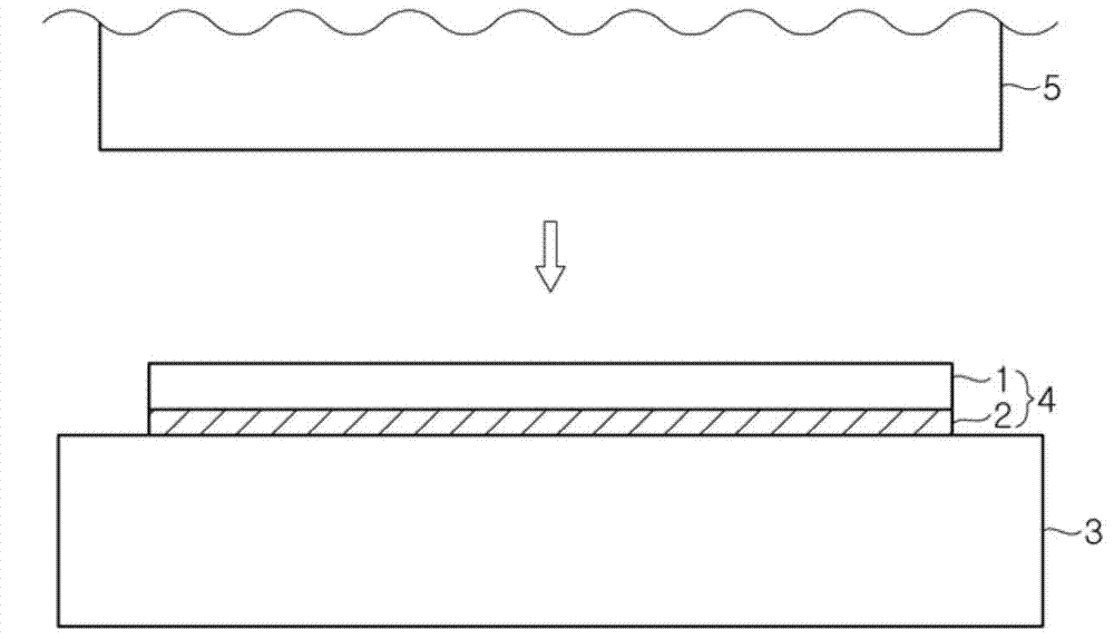
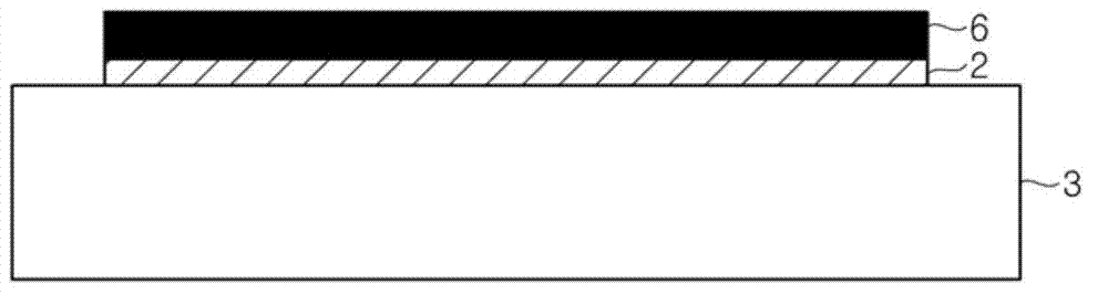
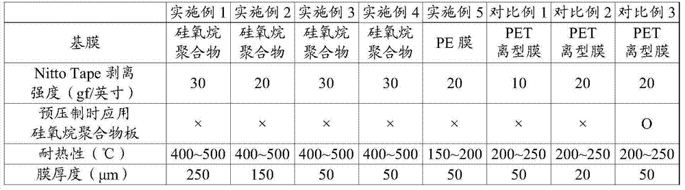
[0032] Example 1: Preparation of anisotropic conductive film

[0033]Based on the parts by weight of the solid content of the following components, 10 parts by weight of butadiene resin, 30 parts by weight of acrylate-modified urethane resin, and 20 parts by weight of acrylic copolymer were mixed, melted and dispersed with a planetary mixer , 36 parts by weight of free radical polymer material, 2 parts by weight of organic peroxide and 2 parts by weight of conductive particles. Then, the mixture was applied to a release-treated 250 μm thick silicone polymer film (storage modulus: 668 kgf / cm 2 ), and dried in a hot air circulation at 60° C. for 5 minutes to dry the solvent, thereby preparing the anisotropic conductive film of Example 1.

[0034] 1. Butadiene resin: acrylonitrile butadiene copolymer (1072CGX, Zeon Chemical Co., Ltd.), which is dissolved in toluene / methyl ethyl ketone at 25vol% (volume percentage);

[0035] 2. Acrylate-modified urethane resin: urethane acrylate...

Embodiment 2

[0040] Embodiment 2: Preparation of anisotropic conductive film

[0041] In addition to using a 150μm thick silicone polymer film (storage modulus: 659kgf / cm 2 ) except that an anisotropic conductive film was prepared in the same manner as in Example 1.

Embodiment 3

[0042] Embodiment 3: Preparation of anisotropic conductive film

[0043] In addition to using a 50μm thick silicone polymer film (storage modulus: 643kgf / cm 2 ) except that an anisotropic conductive film was prepared in the same manner as in Example 1.


PUM

PropertyMeasurementUnit
thicknessaaaaaaaaaa
thicknessaaaaaaaaaa
particle diameteraaaaaaaaaa

Abstract

An anisotropic conductive film, a method for preparing a semiconductor device, and a semiconductor device, the anisotropic conductive film including a base film, the base film having a storage modulus of 5,000 kgf/cm2 or less or a coefficient of thermal expansion of 50 ppm/ DEG C. or less at 100 DEG C to 150 DEG C; and an adhesive layer on the base film, the adhesive layer containing conductive particles.

Description

technical field [0001] The present invention relates to an anisotropic conductive film, its production method, a semiconductor device connected by it, and its production method. Background technique [0002] With the recent trend toward large and thin displays, the pitch between electrodes and lines has become finer. Anisotropic Conductive Film (ACF) plays a very important role as a terminal for connecting delicate circuits. [0003] Methods for Printed Circuit Board (PCB) / Outer Wire Bonding (OLB) and Chip-on-Glass (COG) / Film-on-Glass (FOG) applied to LCD and OLED module processing are divided into those in which ACF is cut into fixed lengths and mounted Pre-press process and main press in which COF, FPC and driver IC are fixed. Due to the pre-pressing process during installation, the failure rate is particularly high, and the main causes of failure include lack of margin for temperature and pressure. Examples of major failures include bubble generation due to wetting fai...

Claims


Application Information

Patent Timeline
Patent Type & Authority Applications(China)
IPC IPC(8): C09J7/02C09J175/14C09J9/02H01L51/52H01L51/56
CPCH01L24/83H01L24/29H01L24/27H01L2224/27001H01L2224/27502H01L2224/2929H01L2224/29355H01L2224/29444H01L2224/32225H01L2224/83101H01L2224/83192H01L2224/83203H01L2224/83851H01L2924/12044H01L2924/14H01L2924/20106Y10T428/266Y10T428/28H01L2924/00H01B1/20H01B5/14H01L23/48
Inventor 崔贤民朴永祐
Owner KUKDO ADVANCED MATERIALS CO LTD
Why Eureka
Try Eureka