Multi-quantum-well structure and light-emitting diode with multi-quantum-well structure

A multi-quantum well structure and quantum well technology, applied in semiconductor devices, electrical components, circuits, etc., can solve the problems of low growth temperature, less polarization charge of quantum wells, and deterioration of quantum well crystal quality

Active Publication Date: 2014-06-18
TIANJIN SANAN OPTOELECTRONICS
View PDF8 Cites 18 Cited by
  • Summary
  • Abstract
  • Description
  • Claims
  • Application Information

AI Technical Summary

Problems solved by technology

However, in this method, the polarization charge of the quantum well in the non-polar or semi-polar surface is very small, the polarization field is small, and the energy band tilt of the quantum well is weakened. Therefore, to achieve the same wavelength, it needs to contain more In components, while the incorporation efficiency of In components on the non-polar and semi-polar surfaces is low, so a lower growth temperature is required, which will deteriorate the crystal quality of the quantum well

Method used


Image

  • Multi-quantum-well structure and light-emitting diode with multi-quantum-well structure
  • Multi-quantum-well structure and light-emitting diode with multi-quantum-well structure
  • Multi-quantum-well structure and light-emitting diode with multi-quantum-well structure

Examples


Embodiment 1

[0027] The following will refer to Figure 1~2 Example 1 of the present invention will be described.

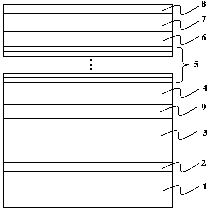
[0028] Please see figure 1 The light emitting diode (LED) structure may sequentially include a substrate 1 , a buffer layer 2 , an N-type conductive layer 3 , a stress release layer 4 , a light emitting region 5 , an electron blocking layer 6 , a P-type conductive layer 7 and a P-type contact layer 8 . Specifically, the substrate 1 can be a sapphire substrate, a gallium nitride substrate or a silicon substrate; the material of the buffer layer 2 is preferably gallium nitride, aluminum nitride material, aluminum gallium nitride material, etc., and the thickness is preferably 30nm; the N-type conductive Layer 3 is preferably gallium nitride, and aluminum gallium nitride material can also be used, and the silicon doping concentration is preferably 2×10 19 cm -3 ; The stress release layer 4 is preferably a superlattice structure in which InGaN / GaN is alternately grown, and the...

Embodiment 2

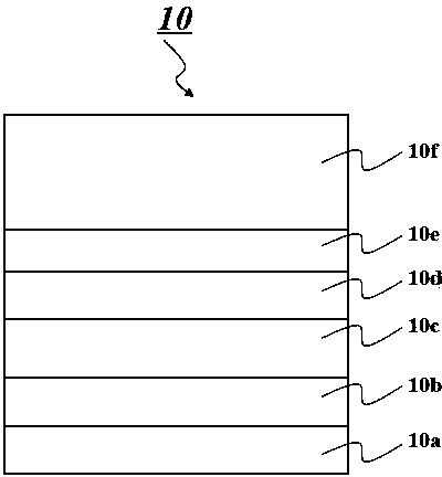
[0046] The following will refer to Image 6 Embodiment 2 illustrating the present invention, Image 6 The light-emitting diode (LED) structure includes a substrate 11, a buffer layer 12 on the substrate 11, an N-type conductive layer 13 on the buffer layer 12, a stress release layer 14 on the N-type conductive layer 13, and The light-emitting region 15 on the stress release layer, the light-emitting region 15 is divided into two parts 15a and 15b. It also includes a P-type electron blocking layer 16 on the light emitting region 15 , a P-type conductive layer 17 on the electron blocking layer 16 , and a P-type contact layer 18 on the P-type conductive layer 17 . In the above structure, except for the light-emitting region 15 , other layer structures and manufacturing methods can refer to the description in Embodiment 1.

[0047] The first part 15 a of the light emitting region 15 includes a periodically repeating structure with nine pairs of quantum well structures 20 and qua...


PUM


Abstract

The invention provides a multi-quantum-well structure and a light-emitting diode with the multi-quantum-well structure. The light-emitting area of the light-emitting diode is provided with at least one quantum well structure comprising a first protection layer, a first transitional layer on the first protection layer, a quantum well layer on the first transitional layer, a second transitional layer on the quantum well layer, a second protection layer on the second transitional layer and a quantum base layer on the second protection layer.

Description

technical field [0001] This invention relates to microelectronic devices and, more particularly, to structures useful in Group III nitride semiconductor devices such as light emitting diodes. Background technique [0002] Light-emitting diodes (LEDs) have the advantages of high brightness, energy saving and environmental protection, and have been recognized as the third-generation lighting source, and have been vigorously developed in recent years. The GaN-based epitaxial wafer grown on the substrate is the core component of the LED and determines the performance of the LED product. [0003] Generally speaking, the LED epitaxial wafer mainly includes a substrate, an N-type conductive layer, a stress release layer, a light-emitting layer, an electron blocking layer, a P-type conductive layer and a P-type contact layer. Among them, the structure and crystal quality of the light-emitting layer play a decisive role in the photoelectric performance of semiconductor devices. In ...

Claims


Application Information

Patent Timeline
Patent Type & Authority Applications(China)
IPC IPC(8): H01L33/06H01L33/00
CPCH01L33/06H01L33/325H01L33/04H01L33/0075H01L33/32
Inventor 刘志彬陈沙沙张东炎刘晓峰王笃祥
Owner TIANJIN SANAN OPTOELECTRONICS
Why Eureka
Try Eureka