Low-power-supply-voltage programmable gain amplifier

A low power supply voltage, programming gain technology, applied in differential amplifiers, DC-coupled DC amplifiers, gain control, etc., can solve the problem of poor linearity and signal-to-noise ratio of analog circuits, can not make up for circuit defects, limit circuit design applications, etc. problems, achieve the effect of reducing power consumption, enriching the circuit structure, and maintaining various performances

Inactive Publication Date: 2014-06-18
SOUTHEAST UNIV
View PDF6 Cites 8 Cited by
  • Summary
  • Abstract
  • Description
  • Claims
  • Application Information

AI Technical Summary

Problems solved by technology

However, for analog circuit designers, since the threshold voltage of the MOS transistor will not decrease proportionally with the size of the transistor, the decreasing power supply voltage will cause the amplitude of the analog signal to decrease, making the linearity and signal-to-noise ratio of the analog circuit change. poor, resulting in a decrease in circuit performance
In order to make up for these defects, the method of increasing the current and bandwidth must be adopted, which will undoubtedly greatly increase the power consumption of the circuit under low power supply voltage, and as the power supply voltage continues to decrease, only increasing the current cannot make up for circuit defects.
In recent years, various low-voltage circuit implementation methods have emerged in the international community, such as double well technology, body drive technology, floating gate transistors, etc., but most of them are based on advanced technology and are expensive, which limits their application in circuit design.

Method used


Image

  • Low-power-supply-voltage programmable gain amplifier
  • Low-power-supply-voltage programmable gain amplifier
  • Low-power-supply-voltage programmable gain amplifier

Examples


Embodiment Construction

[0019] The present invention will be further described below in conjunction with the accompanying drawings.

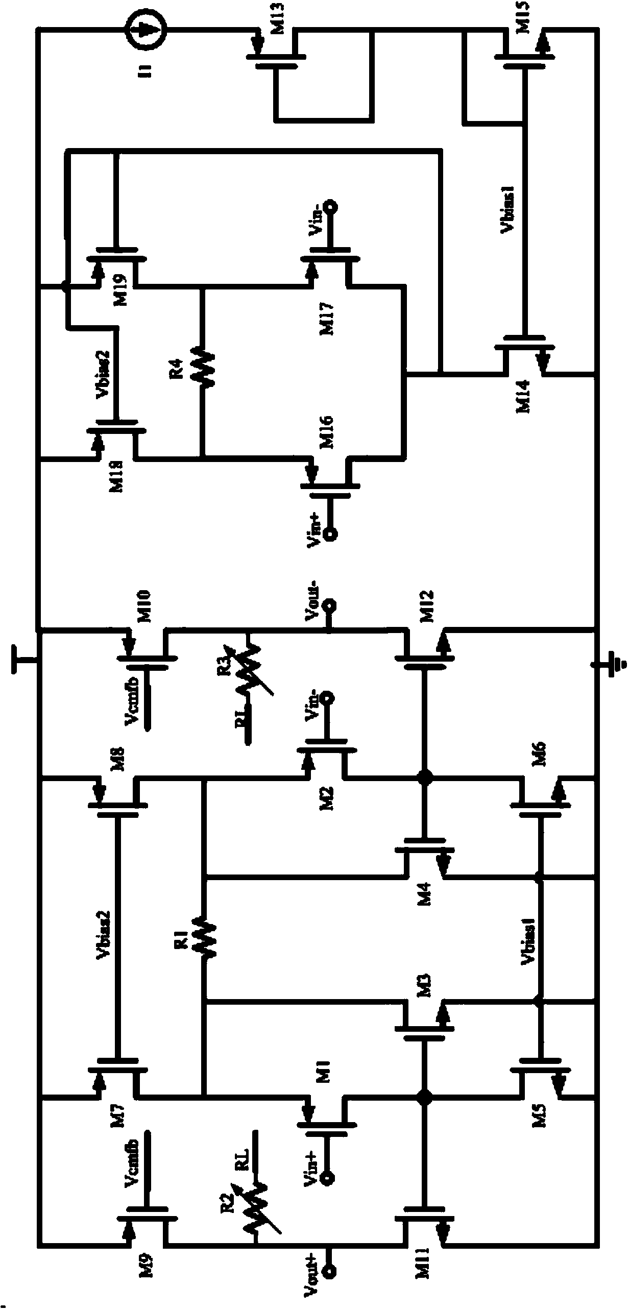
[0020] Such as figure 1 Shown is a programmable gain amplifier with low power supply voltage, which has the characteristics of low power supply voltage for normal operation, which can effectively reduce the power consumption of the circuit. The tail current source of the programmable gain amplifier is biased in the linear region, and a transconductance stage proportional to the differential input transconductance stage is used to form a master-slave structure with the differential input transconductance stage. The tail current source of the master transconductance stage The gate and the gate of the differential input transistor are respectively connected to corresponding ports of the slave transconductance stage in the operational amplifier. Neglecting the channel modulation effect of the transconductance, under the fluctuation of the input voltage or supply voltage, ...


PUM


Abstract

The invention discloses a low-power-supply-voltage programmable gain amplifier. The low-power-supply-voltage programmable gain amplifier comprises a main transconductance stage circuit, a slave transconductance stage circuit and an output stage circuit. A tail current source of the programmable gain amplifier is arranged in a linear region in a bias mode, a transconductance stage and a differential input transconductance stage constitute a main-slave structure and are copied in a proportional mode, and the grid of a main transconductance stage tail current source and the grid of a differential input tube are connected with ports corresponding to slave transconductance stages in an operational amplifier respectively. Based on the main-slave structure, the low-power-supply-voltage programmable gain amplifier is simple in structure and can be realized through standard CMOS technologies; because a transistor is placed on the linear region or a sub-threshold value region in a bias mode, the working power supply voltage of each circuit is further reduced; forms of circuit structures are enriched under the low-power-supply-voltage environment, and the application range of the low-power-consumption programmable gain amplifier is enlarged. Normal work under small voltage is achieved through a simple structure, and therefore power consumption is substantially reduced, and performance can be well kept.

Description

technical field [0001] The invention relates to a low power supply voltage programmable gain amplifier, which belongs to the wireless communication technology. Background technique [0002] In a wireless communication system, due to changes in the surrounding environment or switching of the received channel, the signal strength received by the receiver will change significantly. If the receiving link gain is fixed, nonlinear distortion will easily occur when the input signal strength is high. If the amplifier is in a saturated state or a large signal is blocked, if the input signal is small, the useful signal will be easily overwhelmed by the noise, resulting in the failure of the subsequent circuit to demodulate, that is: if the gain of the receiving link does not vary with the input signal strength For any adjustment, a circuit with a large dynamic range must have excellent noise and linearity performance at the same time, which is often difficult to achieve. Therefore, i...

Claims


Application Information

Patent Timeline
Patent Type & Authority Applications(China)
IPC IPC(8): H03F3/45H03G3/30
Inventor 吴建辉赵超姚红燕黄成李红陈超
Owner SOUTHEAST UNIV
Why Eureka
Try Eureka