Planar optical waveguide type parallel optical assembly and optical module

A planar optical waveguide and optical component technology, applied in the field of optical communication, can solve the problems of increasing the electrical parasitic effect of optical components, limiting the transmission rate of the system, and high manufacturing cost, and achieving the effects of reducing electrical parasitic effect, simple coupling structure and low cost

Inactive Publication Date: 2014-06-25
SHENZHEN NEOPHOTONICS TECH
View PDF6 Cites 13 Cited by
  • Summary
  • Abstract
  • Description
  • Claims
  • Application Information

AI Technical Summary

Problems solved by technology

This scheme adopts more components, the process is more complicated, and the manufacturing cost is high
The use of flexible circuit boards an...

Method used


Image

  • Planar optical waveguide type parallel optical assembly and optical module
  • Planar optical waveguide type parallel optical assembly and optical module
  • Planar optical waveguide type parallel optical assembly and optical module

Examples


Embodiment 1

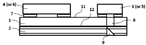
[0032] Such as figure 1 and figure 2 As shown, the planar optical waveguide type parallel optical component of this embodiment includes a circuit board 1 , an optical waveguide 2 , a laser array 3 , a driver 4 , an optical detector array 5 and a transconductance amplifier 6 . Both the laser array 3 and the photodetector array 5 are four parallel arrays. The laser in this embodiment is a vertical cavity surface emitting laser (VCSEL).

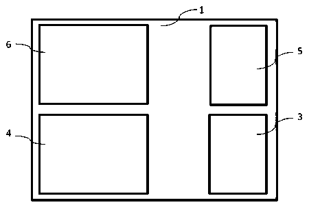
[0033] An electrode array 7 is arranged on the first side 11 of the circuit board 1, and the VCSEL array 3, the driver 4, the photodetector array 5 and the transconductance amplifier 6 are mounted on the first side of the circuit board 1 in a flip-chip bonding manner. side 11 and is electrically connected to the electrode array 7 . The arrangement of the VCSEL array 3, driver 4, photodetector array 5 and transconductance amplifier 6 on the circuit board 1 is as follows: figure 2 shown.

[0034] Such as figure 1 As shown, the light-transm...

Embodiment 2

[0039] The difference between this embodiment and Embodiment 1 is that the light-transmitting device provided on the circuit board 1 is realized by using a transparent substrate, such as Figure 4 shown. In this embodiment, the transparent substrate is a polyimide film. The polyimide film is selected as the transparent substrate of the circuit board, and its transmittance to the 850nm near-infrared light emitted by the VCSEL can reach more than 85%. The thickness of the polyimide film in this embodiment is 30 microns. The circuit board 1 itself has a multilayer circuit. Using transparent polyimide film as the substrate of the circuit board can save the drilling procedure, thereby reducing the cost.

[0040] Such as figure 2 and Figure 4 As shown, the planar optical waveguide type parallel optical component of this embodiment includes a circuit board 1 , an optical waveguide 2 , a laser array 3 , a driver 4 , an optical detector array 5 and a transconductance amplifier 6...

Embodiment 3

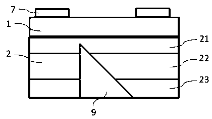
[0046] The difference between this embodiment and Embodiment 1 is that the polymer film of the optical waveguide 2 is hot-pressed on the circuit layer by layer with the first cladding layer 11, the core layer 2, and the second cladding layer 13 by dry film lamination. plate 1. Firstly, the first cladding layer 11 is made on the circuit board 1, and the dry film of the core layer 12 is hot-pressed, and the core layer 12 is exposed and developed according to the preset optical path pattern to form the wiring of the optical signal channel, Then press the second cladding layer 13 , that is, the upper cover layer of the waveguide to fill the gaps in the wiring. The polymer film in this embodiment is formed by mixing oligomers and polymer resins. Preferably, an ultraviolet curable oligomer can be used.

[0047] The polymer film formed by mixing oligomer and polymer resin has a small bending radius, which can be about 3 mm. After repeated bending and folding, the optical loss incre...


PUM

PropertyMeasurementUnit
Thicknessaaaaaaaaaa
Thicknessaaaaaaaaaa
Thicknessaaaaaaaaaa

Abstract

Disclosed in the invention is a planar optical waveguide type parallel optical assembly comprising a circuit board, an optical waveguide, a laser array, a driver, an optical detector array and a transconductance amplifier. A photoelectric chip is installed at a first side of the circuit board in a back bonding mode. A light-transmitting device is arranged at the circuit board; and the optical waveguide is contacted to a second side of the circuit board and contains a 45-degree mirror surface. In addition, the invention also discloses a planar optical waveguide type parallel optical module. With the planar optical waveguide type parallel optical assembly and optical module, the bandwidth density of optical interconnection is improved; and the process based on the photoelectric integration scheme is simple, so that large-scale production can be realized beneficially. The photoelectric chip is installed by using the back bonding technique, thereby effectively reducing an electric parasitic effect. The light path enters the optical waveguide by a bending way and is directly coupled to a pluggable interface of the parallel fiber, so that the lens is not needed; the less optical elements are used, the coupling structure is simple, and the cost is low. The polymer film is used for manufacturing the optical waveguide; the bending radius is small; and the maneuverability is enhanced.

Description

technical field [0001] The invention relates to the field of optical communication, in particular to a planar optical waveguide type parallel optical assembly and an optical module. Background technique [0002] The optical transceiver module market has experienced unprecedented growth in the past decade, and optical transceiver modules are widely used in the fields of telecommunications and data communications. With the increase of bandwidth requirements, the requirements for miniaturization of form factor and low power consumption are further advanced, and people pay more attention to space energy efficiency and port rate density. The miniaturized parallel optical fiber interconnection scheme can achieve unlimited expansion of bandwidth by adding parallel data transmission channels. Parallel optical interconnection has gradually become a standard solution for data centers and high-performance computer installations, and active optical cables containing two high-speed para...

Claims


Application Information

Patent Timeline
IPC IPC(8): G02B6/43
Inventor 侯小珂张胜利
Owner SHENZHEN NEOPHOTONICS TECH
Why Eureka
Try Eureka