Texture etching solution composition and texture etching method of crystalline silicon wafers

A composition and etching solution technology, applied in the direction of surface etching composition, chemical instrument and method, climate sustainability, etc., can solve problems such as productivity and cost uneconomical, large deviation of texture quality, poor pyramid formation, etc. , to achieve the effect of process cost economy, reduce reflectivity, improve quality and productivity

Inactive Publication Date: 2014-06-25
DONGWOO FINE CHEM CO LTD
View PDF14 Cites 11 Cited by
  • Summary
  • Abstract
  • Description
  • Claims
  • Application Information

AI Technical Summary

Problems solved by technology

However, this etching method has the following disadvantages: it not only causes poor pyramid formation, but also causes an increase in light reflectivity and a decrease in efficiency, and requires additional ventilation.
However, these etching solutions all contain isopropanol with a relatively low boiling point. Since this isopropanol must be supplemented in the texturing process, it is not economical in terms of productivity and cost, and the isopropanol due to the supplementary input is reduced. The temperature gradient of the etching solution occurs, resulting in a large deviation in the quality of the texture at different positions on the surface of the silicon wafer, which may affect the uniformity

Method used


Image

  • Texture etching solution composition and texture etching method of crystalline silicon wafers
  • Texture etching solution composition and texture etching method of crystalline silicon wafers
  • Texture etching solution composition and texture etching method of crystalline silicon wafers

Examples


Embodiment 1~20 and comparative example 1~6

[0089] In accordance with the components and composition ratios (% by weight) described in Table 1 below, the remainder of water was added to prepare an etchant composition for texturing a crystalline silicon wafer.

[0090] [Table 1]

[0091]

[0092]

[0093]

experiment example

[0095] Single crystal silicon wafers were immersed in the etching liquid compositions for texture of crystalline silicon wafers of Examples 1 to 20 and Comparative Examples 1 to 6, respectively, and etched. The texture conditions at this time were a temperature of 80° C. and a time of 20 minutes.

[0096] The uniformity and reflectance of the texture formed by each composition were measured, and the results are shown in Table 2.

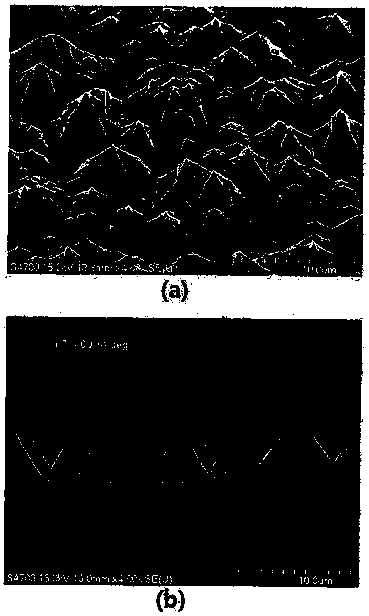
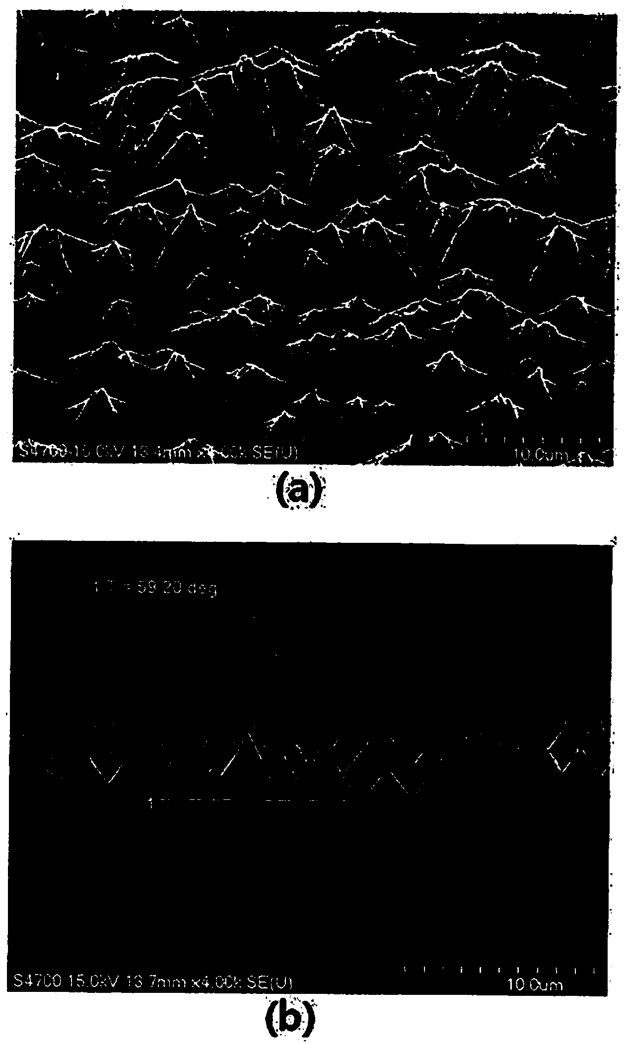
[0097] in addition, figure 1 It is an SEM photograph showing the texture of a single crystal silicon wafer etched using the etching solution composition for texture of a crystalline silicon wafer in Example 1, figure 2 It is a SEM photograph showing the texture of a single crystal silicon wafer etched using the etching solution composition for texture of a crystalline silicon wafer in Example 13,

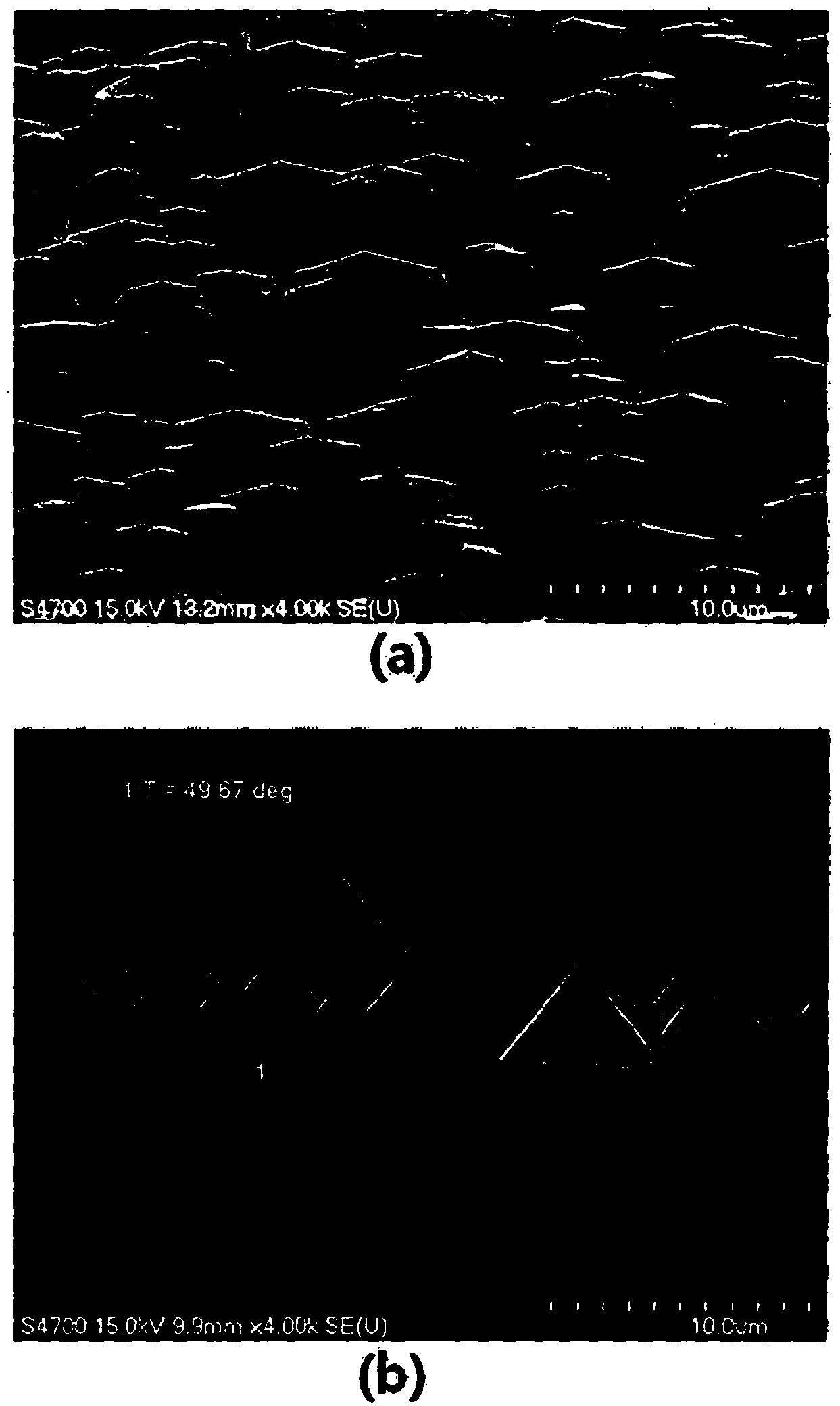
[0098] image 3 This is an SEM photograph showing the texture of a silicon single crystal wafer etched with the etching solution composition for textu...


PUM

PropertyMeasurementUnit
boiling pointaaaaaaaaaa
electrical resistivityaaaaaaaaaa

Abstract

Disclosed are a texture etching solution composition for a crystalline silicon wafer, and a texture etching method using the same. The texture etching solution composition for a crystalline silicon wafer includes a polymer formed by polymerizing a monomer that is substituted with a cyclic compound having 4 to 10 carbon atoms as well as at least one nitrogen atom. The texture etching solution composition and the texture etching method are capable of forming pyramids with a specific structure which can minimize a quality deviation of a texture within a region in formation of a micro-pyramid structure on the surface of the crystalline silicon wafer to increase luminous efficiency while reducing a reflectivity.

Description

technical field [0001] The invention relates to a texture etching liquid composition and a texture etching method for a crystalline silicon wafer, which can minimize the quality deviation of textures at different positions on the surface of the crystalline silicon wafer and improve light efficiency. Background technique [0002] In recent years, a solar cell, which has rapidly spread as a next-generation energy source, is an electronic component that directly converts solar energy, a clean energy, into electric energy, and is composed of a PN junction semiconductor substrate in which boron is added to The P-type silicon semiconductor in silicon is used as a substrate, and phosphorus is diffused on the surface to form an N-type silicon semiconductor layer. [0003] When light such as sunlight is irradiated on the substrate where the electric field is formed by the PN junction, the electrons (-) and holes (+) in the semiconductor are excited and become a state of free movement...

Claims


Application Information

Patent Timeline
Patent Type & Authority Applications(China)
IPC IPC(8): C09K13/00H01L31/18
CPCY02P70/50
Inventor 洪亨杓李在连朴勉奎林大成
Owner DONGWOO FINE CHEM CO LTD
Why Eureka
Try Eureka