Ultrathin nanosheet semiconductor material and preparation method and application thereof

A nanosheet and semiconductor technology, applied in nanotechnology, nanotechnology, nanotechnology for materials and surface science, etc., can solve the problems of low yield of semiconductor materials, complex equipment and conditions, high investment, etc., and achieve effective absorption and utilization, low cost, and the effect of overcoming large energy consumption

Active Publication Date: 2014-07-02
UNIV OF SCI & TECH OF CHINA
View PDF5 Cites 18 Cited by
  • Summary
  • Abstract
  • Description
  • Claims
  • Application Information

AI Technical Summary

Problems solved by technology

The high-temperature vapor phase method includes methods such as vapor deposition and molecular beam epitaxy. Its advantage is that it can synthesize ultra-thin nanosheet semiconductor materials with extremely low thickness. The required equipment and conditions are very complicated and the investment is high

Method used


Image

  • Ultrathin nanosheet semiconductor material and preparation method and application thereof
  • Ultrathin nanosheet semiconductor material and preparation method and application thereof
  • Ultrathin nanosheet semiconductor material and preparation method and application thereof

Examples


preparation example Construction

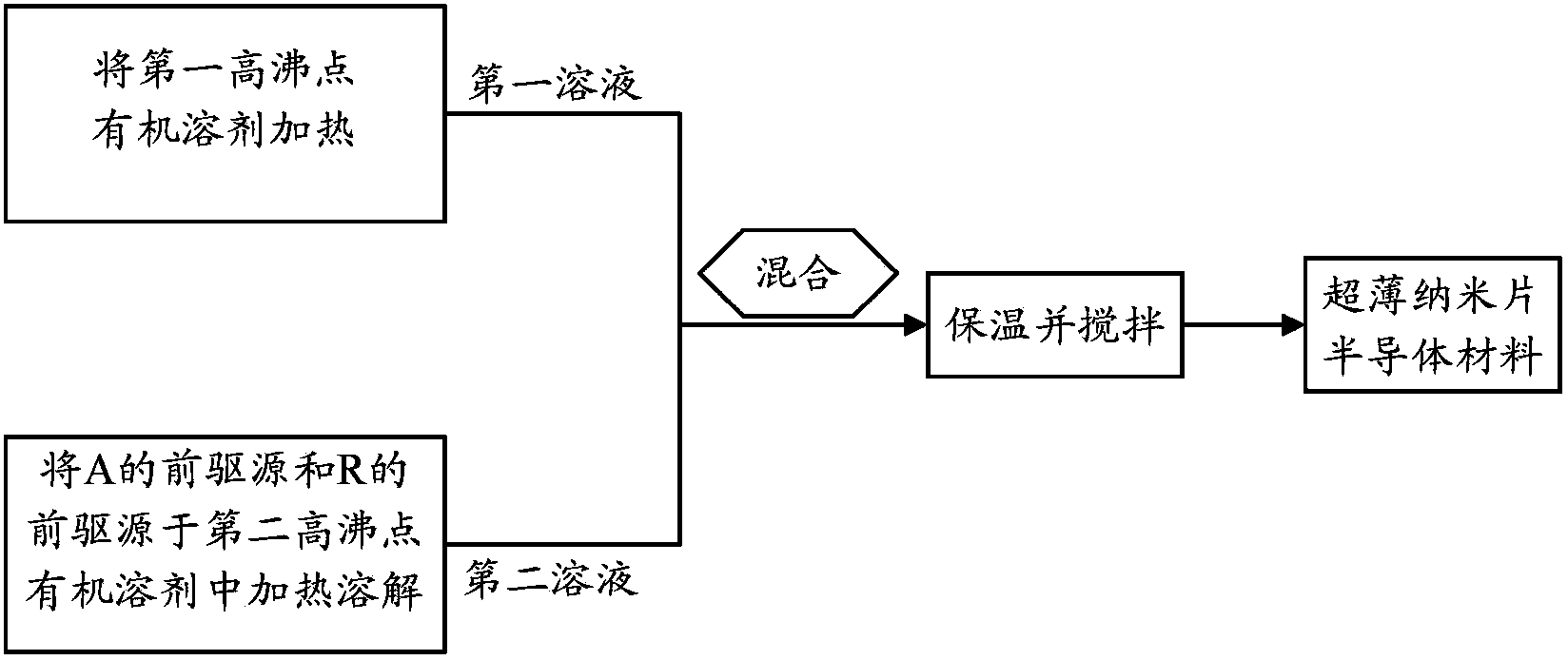
[0033] Such as figure 1 As shown, the invention discloses a method for preparing an ultra-thin nanosheet semiconductor material, comprising the following steps:

[0034] Step 1: heating the first high boiling point organic solvent to obtain the first solution. This step can provide a reaction solvent with a certain temperature, and the purpose of heating is to fully remove the moisture and oxygen in the first high-boiling point organic solvent. Preferably, the heating temperature is 200-320°C, and the first high-boiling-point organic solvent can be selected from one or more of oleylamine, oleic acid, dibenzylamine, dibenzyl ether, octadecene and diisooctylamine , wherein the volume of the first high-boiling organic solvent does not need to be strictly controlled, but for the convenience of operation, it can be proportional to the volume of the second high-boiling organic solvent in the second step.

[0035] In order to heat more evenly and fully isolate oxygen and water vapo...

Embodiment 1

[0045] In a 50mL three-neck flask, add 15.0ml oleylamine and 15.0ml oleic acid, heat to 180°C at a heating rate of 20°C / min, keep it warm for 1 hour, and then heat to 320°C at a heating rate of 20°C / min to obtain the first solution; add 0.1mmol phenyl bismuth and 0.2mmol phenyl selenium to 10ml of oleylamine solution and heat at 60°C until completely dissolved to obtain the second solution; mix the first solution and the second solution and heat at 300°C Under stirring for 20min, the final product was washed and sonicated to obtain the ultrathin nanosheet Bi 2 Se 3 .

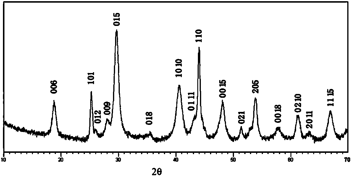
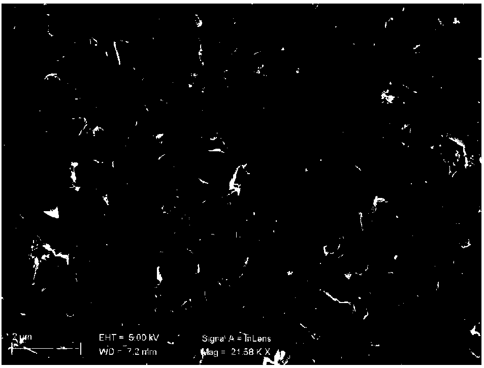
[0046] Such as Figure 2 to Figure 6 As shown, the product is a single crystal ultrathin nanosheet Bi with a thickness of about 1 nm 2 Se 3 Material. Photothermal performance tests show that the prepared ultrathin nanosheets Bi 2 Se 3 The photothermal conversion power is greater than 8W / g, which is not lower than the conversion efficiency of activated carbon under the same conditions. In ultra-thin nanoma...

Embodiment 2

[0048] In a 50mL three-neck flask, add 5.0ml of dibenzylamine, heat it to 150°C at a heating rate of 10°C / min, keep it warm for 30min, and then heat it to 300°C at a heating rate of 15°C / min to obtain the first solution; Add mmol phenyl bismuth and 0.2 mmol phenyl selenium to 0.1 ml of dibenzylamine solution and heat at 100°C until completely dissolved to obtain the second solution; mix the first solution and the second solution and stir at 250°C 100min, wash and sonicate the final product to obtain the ultrathin nanosheet Bi 2 Se 3 .

[0049] The properties of the resulting product were tested, and the product was a single-crystal ultrathin nanosheet Bi with a thickness of about 1 nm. 2 Se 3 Material. Photothermal performance tests show that the prepared ultrathin nanosheets Bi 2 Se 3 The photothermal conversion power is greater than 8W / g, which is not lower than the conversion efficiency of activated carbon under the same conditions. In ultra-thin nanomaterials, its si...


PUM

PropertyMeasurementUnit
Thicknessaaaaaaaaaa

Abstract

The invention provides an ultrathin nanosheet semiconductor material and a preparation method and application thereof. The preparation method comprises the following steps: heating a first organic solvent with high boiling point to obtain a first solution; heating to dissolve a precursor source AnBm of an A and a precursor source RjVk of an R in a second organic solvent with high boiling point to obtain a second solution; and mixing the first solution and the second solution, and heating with stirring to obtain the ultrathin nanosheet semiconductor material. The invention has the advantages of simple preparation process, good repeatability and strong controllability; the prepared nanometer material has thickness of 1-50 nm and an ultrathin nanosheet structure; and the ultrathin nanosheet semiconductor material prepared by the invention has photothermal conversion effect, and can be used as a novel photothermal conversion material in a solar cell or a solar energy collection device.

Description

technical field [0001] The invention relates to the field of preparation of solid inorganic materials, in particular to an ultra-thin nanosheet semiconductor material and its preparation method and application. Background technique [0002] Ultrathin nanosheet semiconductor material is an important thermoelectric material, which has important application prospects in optics, optoelectronic science and its devices, as well as energy conversion and utilization, such as ultrathin Bi 2 Se 3 and Bi 2 Te 3 Such semiconductor materials have greater thermoelectric conversion efficiency than similar bulk materials, and can also form two-dimensional topological insulators, and when ultrathin Bi 2 Se 3 and Bi 2 Te 3 and other semiconductor materials and TaSe 2 and TaTe 2 Superconductors with higher critical temperatures can also be formed when superlattice structures are formed. [0003] In recent years, it has been found that ultrathin nanosheet semiconductor materials not on...

Claims


Application Information

Patent Timeline
IPC IPC(8): C01B19/04B82Y30/00
CPCY02P20/133
Inventor 杨晴周俊周晓丽王文亮陆亚林
Owner UNIV OF SCI & TECH OF CHINA
Why Eureka
Try Eureka