Method for reducing ohmic contact resistance of HEMT device

A technology of ohmic contact and resistance, applied in semiconductor devices, semiconductor/solid-state device manufacturing, circuits, etc., can solve problems such as surface topography and edge uniformity, GaN material damage, etc.

Inactive Publication Date: 2014-07-02
THE 13TH RES INST OF CHINA ELECTRONICS TECH GRP CORP
View PDF3 Cites 8 Cited by
  • Summary
  • Abstract
  • Description
  • Claims
  • Application Information

AI Technical Summary

Problems solved by technology

However, judging from the existing results, the above-mentioned methods all require high-temperature alloys, and the surface morphology and edge regularity after alloying are not ideal and need to be improved.
In addition, there is also ion implantation through the source and drain regions to achieve low ohmic contact and good surface morphology, but this process requires high temperature to activate the implanted ions, and there will be lateral diffusion during the implantation process, causing damage to the GaN material

Method used


Image

  • Method for reducing ohmic contact resistance of HEMT device
  • Method for reducing ohmic contact resistance of HEMT device
  • Method for reducing ohmic contact resistance of HEMT device

Examples


Embodiment 1

[0038] In this embodiment, the AlGaN / GaN HEMT device material is taken as an example, and the implementation mode of the present invention is described in detail in conjunction with the accompanying drawings:

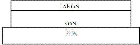
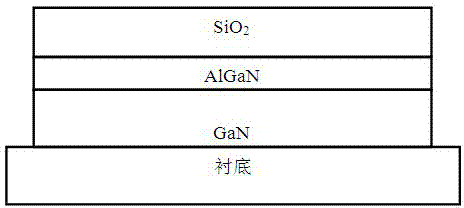
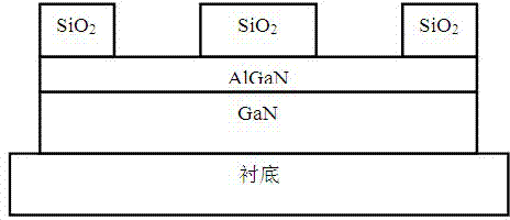
[0039] figure 1 It is a schematic diagram of the general structure of AlGaN / GaN HEMT device materials; 150nm silicon dioxide (SiO2) is grown on the surface of AlGaN / GaN materials 2 ),Such as figure 2 Shown; using reactive ion etching equipment (RIE) to etch SiO in the source and drain ohmic regions of HEMT devices 2 layer to the upper surface of the AlGaN barrier layer, such as image 3 As shown; use inductively coupled plasma etching equipment (ICP) to etch the GaN material in the ohmic region of the source and drain of the HEMT device, and etch to below the AlGaN / GaN heterojunction interface (the etching depth is about 40nm), as Figure 4 Shown; above steps can be realized by prior art.

[0040] The inventive point of the present invention is that after secondar...

Embodiment 2

[0044] In this embodiment, taking the InAlN / GaN HEMT device material as an example, the implementation of the present invention is described in detail:

[0045] Growth of 200nm silicon dioxide (SiO2) on the surface of InAlN / GaN material 2 ) layer; use reactive ion etching equipment (RIE) to etch SiO in the source and drain ohmic regions 2 Layer to the upper surface of the InAlN barrier layer; use inductively coupled plasma etching equipment (ICP) to etch the GaN material in the ohmic region of the source and drain of the HEMT device, etch below the InAlN / GaN heterojunction interface (the etching depth is about 30nm ); the above steps can be realized by prior art.

[0046] Then, use MOCVD equipment to epitaxially secondarily 60nm n-type heavily doped GaN material in the source-drain ohmic region after the treatment of the above device; and then anneal in a high-temperature annealing furnace at 300°C for 3 minutes in a high-purity nitrogen atmosphere to obtain the obtained req...

Embodiment 3

[0048] In this embodiment, an InAlN / GaN HEMT device material is taken as an example to describe the implementation of the present invention in detail. In this embodiment, the focus is on the adjustment of process parameters.

[0049] Growth of 200nm silicon dioxide (SiO2) on the surface of InAlN / GaN material 2 ) layer; use reactive ion etching equipment (RIE) to etch SiO in the source and drain ohmic regions 2 Layer to the upper surface of the InAlN barrier layer; use inductively coupled plasma etching equipment (ICP) to etch the GaN material in the ohmic region of the source and drain of the HEMT device, etch below the InAlN / GaN heterojunction interface (the etching depth is about 50nm ); the above steps can be realized by prior art. Then, use MOCVD equipment to epitaxially secondarily 60nm n-type heavily doped GaNN material in the source-drain ohmic region after the above-mentioned device processing; and then anneal in a high-temperature annealing furnace at 800°C for 0.5 m...


PUM

PropertyMeasurementUnit
thicknessaaaaaaaaaa
thicknessaaaaaaaaaa

Abstract

The invention discloses a method for reducing the ohmic contact resistance of an HEMT device and relates to the technical field of methods for preparing nitride. The method comprises the steps that (1) an extension structure grows and a GaN layer and a barrier layer are formed on a substrate in sequence; (2) a SiO2 layer grows on the upper surface of the barrier layer; (3) the SiO2 layer is etched to the upper surface of the barrier layer in a drain-source ohm zone; (4) a GaN material is etched in a source-drain ohm zone and etched to the portion below a heterojunction interface of the GaN layer and the barrier layer; (5) secondary extension is conducted on an n-type heavy doping GaN material in the source-drain ohm zone; (6) SiO2 remaining on the upper surface of the barrier layer is etched off and annealing treatment is conducted through a high-temperature annealing furnace in a pure nitrogen atmosphere or a vacuum atmosphere. According to the method, ohmic contact between the n-type heavy doping GaN and a GaN heterojunction side wall is improved and the contact resistance of the n-type heavy doping GaN and the GaN heterojunction side wall is reduced.

Description

technical field [0001] The invention relates to the technical field of preparation methods of nitrides, in particular to a method for reducing the ohmic contact resistance of HEMT devices. Background technique [0002] As a representative of the third-generation semiconductor material, GaN material is an important semiconductor material after Si and GaAs materials. Because of its large forbidden band width, high critical field strength, high carrier saturation velocity and high temperature and radiation resistance Lighting and other excellent properties have attracted widespread attention. Among them, GaN-based heterojunction (such as AlGaN / GaN and InAl / GaN, etc.) High Electron Mobility Field Effect Transistor (HEMT) has demonstrated excellent performance in the microwave and millimeter wave fields, which has led to extensive and in-depth research at home and abroad. After years of efforts, the performance and stability of GaN-based HEMT devices have been greatly improved. ...

Claims


Application Information

Patent Timeline
Patent Type & Authority Applications(China)
IPC IPC(8): H01L21/335H01L21/28
CPCH01L21/28575H01L29/66462
Inventor 吕元杰冯志红顾国栋郭红雨尹甲运敦少博
Owner THE 13TH RES INST OF CHINA ELECTRONICS TECH GRP CORP
Why Eureka
Try Eureka