Manufacturing method of gate dielectric layer

A technology of gate dielectric layer and manufacturing method, which is applied in the manufacture of semiconductor/solid-state devices, electrical components, circuits, etc., can solve the problems of negative impact on carrier migration speed, volatilization of nitrogen elements on the surface, etc., and reduce threshold voltage drift. Stabilized risk, stable nitrogen content, effect of high dielectric constant

Inactive Publication Date: 2014-07-02
SHANGHAI HUALI MICROELECTRONICS CORP
View PDF2 Cites 7 Cited by
  • Summary
  • Abstract
  • Description
  • Claims
  • Application Information

AI Technical Summary

Problems solved by technology

[0017] In the above preparation process, since the doped nitrogen element has a high concentration and is mainly distributed on the upper surface of the gate dielectric, the temperature, gas atmosphere and time interval of the subsequent high-temperature annealing process (PNA, Post Nitriding Anneal) must be strictly controlled , to prevent the influence of the intrinsic oxide layer and organic adsorption on nitrogen doping; in addition, the subsequent high-temperature annealing process can easily cause the volatilization of nitrogen on the surface, and enable nitrogen to gain energy and continue to diffuse, causing some nitrogen to Accumulated on SiO 2 / Si interface, thus negatively affecting the mobility of carriers in the channel

Method used


Image

  • Manufacturing method of gate dielectric layer

Examples


Embodiment Construction

[0038]The problem to be solved by the present invention is to provide a method for fabricating a gate dielectric layer. The formed gate dielectric layer has a relatively high dielectric constant and can effectively suppress the diffusion of impurities in the gate dielectric layer.

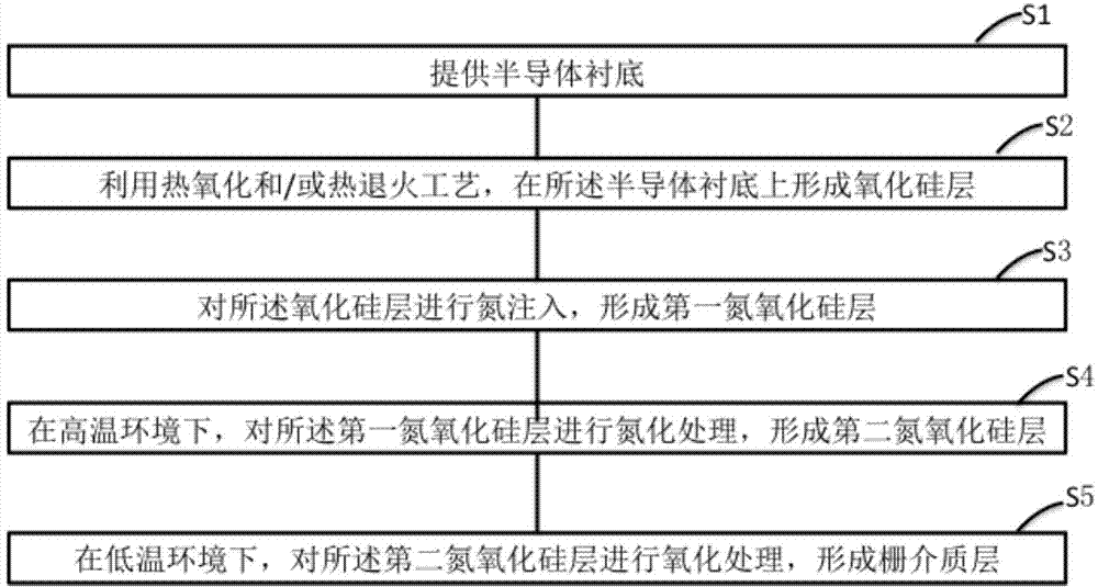
[0039] In order to solve the above problems, the present invention provides a method for fabricating a gate dielectric layer, please refer to figure 1 Shown is a schematic flow chart of a method for manufacturing a gate dielectric layer according to an embodiment of the present invention. The method for manufacturing a gate dielectric layer of the present invention includes:

[0040] Step S1, providing a semiconductor substrate;

[0041] Step S2, using a thermal oxidation and / or thermal annealing process to form a silicon oxide layer on the semiconductor substrate;

[0042] Step S3, performing nitrogen implantation on the silicon oxide layer to form a first silicon oxynitride layer;

[0043] Step...


PUM

PropertyMeasurementUnit
relative permittivityaaaaaaaaaa

Abstract

The invention provides a manufacturing method of a gate dielectric layer. The manufacturing method comprises the steps that a semiconductor substrate is provided; a silicon oxide layer is formed on the semiconductor substrate by using a thermal oxidation technology and / or a thermal annealing technology; nitride injection is conducted on the silicon oxide layer to form a first silicon oxynitride layer; under high-temperature environment, nitriding processing is conducted on the first silicon oxynitride layer to form a second silicon oxynitride layer; under low-temperature environment, oxidizing processing is conducted on the second silicon oxynitride layer to form the gate dielectric layer. The gate dielectric layer formed through the method has a higher dielectric constant, and meanwhile can effectively prevent impurities from dispersing in the gate dielectric layer.

Description

technical field [0001] The invention relates to a manufacturing process for semiconductor MOS devices, more precisely, the invention relates to a method for preparing a gate dielectric layer. Background technique [0002] The rapid development of Very Large Scale Integration (VLSI) and Ultra Large Scale Integration (ULSI) has put forward more special requirements for device processing technology. Among them, the requirement for the gate dielectric layer when the feature size of MOS devices enters the nanometer era is an obvious challenge. The preparation process of the gate dielectric layer is a key technology in the semiconductor manufacturing process, which directly affects and determines the electrical characteristics and reliability of the device. [0003] The key performance indicator of MOSFET devices is the drive current, and the magnitude of the drive current depends on the gate capacitance. The gate capacitance is proportional to the surface area of ​​the gate and ...

Claims


Application Information

Patent Timeline
Patent Type & Authority Applications(China)
IPC IPC(8): H01L21/336H01L21/28
CPCH01L21/28158H01L21/28185H01L21/28211
Inventor 张红伟
Owner SHANGHAI HUALI MICROELECTRONICS CORP
Why Eureka
Try Eureka