
Low-power-consumption thin back gate graphene field effect transistor manufacturing method

A technology of field effect transistors and graphene, which is applied in the direction of transistors, semiconductor/solid-state device manufacturing, semiconductor devices, etc., can solve the problems of high power consumption and large input voltage, and achieve low power consumption, reduce power consumption, and promote development. Effect

Inactive Publication Date: 2014-07-23
JIANGSU UNIV
View PDF2 Cites 7 Cited by
  • Summary
  • Abstract
  • Description
  • Claims
  • Application Information

AI Technical Summary

Problems solved by technology

According to Moore's Law, every 18 to 24 months, the transistor density of integrated circuits doubles and the operating frequency doubles, but the power consumption also doubles, which has become the biggest bottleneck of Moore's Law, so the design and manufacture of ultra-low power consumption Nanoelectronic components are an urgent problem to be solved today
At present, the common back-gate graphene field-effect transistors are all based on 300nm thick SiO 2 As a gate dielectric layer, its input voltage is relatively large, and its power consumption is relatively large

Method used


Image

  • Low-power-consumption thin back gate graphene field effect transistor manufacturing method
  • Low-power-consumption thin back gate graphene field effect transistor manufacturing method
  • Low-power-consumption thin back gate graphene field effect transistor manufacturing method

Examples


Embodiment Construction

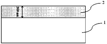
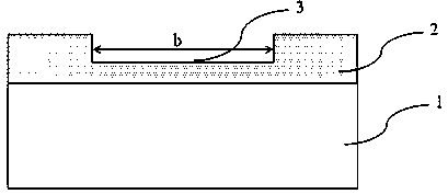
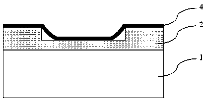
[0016] When the gate oxide of the field effect transistor is 300 nm, the gate voltage range required for its transfer characteristics is about -150~150 V, which is a very large span, which is not suitable for the power consumption of general micro-nano electronic devices. For sensors based on graphene field-effect transistors, it is desirable to control the input voltage within the range of 5 V, which is conducive to the application of portable graphene devices. In order to ensure the performance of the graphene field effect transistor and provide sufficient current drive when the gate voltage is reduced, it is necessary to reduce the thickness of the gate oxide, so reactive ion etching technology is used to obtain a thin gate oxide.

[0017] see figure 1 , thermally grow 300 nm thick SiO on the surface of n-type Si substrate 1 with a resistivity of 1~10 Ωcm 2 Medium layer 2. see figure 2 , using mask No. 1 for SiO 2 Dielectric layer 2 is subjected to photolithography, an...


PUM

PropertyMeasurementUnit
Resistivityaaaaaaaaaa
Thicknessaaaaaaaaaa

Abstract

The invention discloses a low-power-consumption thin back gate graphene field effect transistor manufacturing method. A SiO2 dielectric layer is grown on the surface of an n-type Si substrate through heat, the SiO2 dielectric layer is subjected to photoetching, the SiO2 dielectric layer is etched with reactive ions after development, grooves are formed, graphene is transferred to the etched SiO2 dielectric layer, graphene channels are formed, TiW alloy with the thickness of 5 nm and Au with the thickness of 100 nm are sequentially arranged on the surfaces of the graphene channels in a sputtering mode, then, photoetching is performed, the TiW / Au is corroded to form a linear Au connecting wire and an Au electrode plate after development, a source electrode and a drain electrode are formed, and the purpose of low power consumption and the purpose of high performance are effectively achieved.

Description

technical field [0001] The invention belongs to the technical field of nanoelectronic components and relates to a method for preparing a low-power consumption thin back-gate graphene field-effect transistor. Background technique [0002] Field-effect transistors (FETs) are the most important devices in very large-scale integrated circuits such as microprocessors and semiconductor memories. FET through the gate-source voltage ( V gs ) to control the conductivity of the channel, so as to control the output current ( I ds ) size purposes. As a high-speed response device, FET must respond quickly to changing gate-source voltage, so it needs to have a small gate and a conductive channel with high carrier mobility. [0003] In 2004, condensed matter physicists discovered a graphene that is only a few atomic layers thick at room temperature. This material is composed of carbon atoms with sp 2 The hybrid orbitals form a hexagonal planar film with a honeycomb lattice, and its ...

Claims


Application Information

Patent Timeline
IPC IPC(8): H01L21/336H01L21/28
CPCH01L29/66045H01L29/42364
Inventor 王权刘帅任乃飞李允祝俊王雯张腾飞
Owner JIANGSU UNIV
Learn More