Organic semiconductor material, preparation method and electroluminescent device

A technology of electroluminescent devices and organic semiconductors, applied in the direction of semiconductor devices, semiconductor/solid-state device manufacturing, organic compound preparation, etc., can solve problems such as shortages, and achieve the effects of reduced manufacturing costs, reduced process flow, and cheap raw materials

Inactive Publication Date: 2014-08-06
OCEANS KING LIGHTING SCI&TECH CO LTD +2
View PDF2 Cites 4 Cited by
  • Summary
  • Abstract
  • Description
  • Claims
  • Application Information

AI Technical Summary

Problems solved by technology

However, there are few efficient blue phosphorescent devices, mainly due to the lack of both good carrier transport performance and high triplet energy level (E T ) of the host material

Method used


Image

  • Organic semiconductor material, preparation method and electroluminescent device
  • Organic semiconductor material, preparation method and electroluminescent device
  • Organic semiconductor material, preparation method and electroluminescent device

Examples


preparation example Construction

[0025] The present invention provides a method for preparing an organic semiconductor material, including the following steps:

[0026] Provide compound A: And compound B: Where R is C 1 ~C 20 In an inert atmosphere, compound A and compound B are added into an organic solvent containing a catalyst and an alkali solution in a molar ratio of 1:1 to 1:1.2, and the Suzuki coupling reaction is carried out at 70 to 130 ℃ 12~ For 96 hours, the catalyst is organopalladium or a mixture of organopalladium and organophosphorus ligand, to obtain an organic semiconductor material P represented by the following structural formula:

[0027] Wherein, n is an integer from 10 to 100.

[0028] In a specific embodiment, the method for preparing the organic semiconductor material further includes a step of separating and purifying the organic semiconductor material P, and the step of separating and purifying is as follows: the compound A and the compound B are subjected to the Suzuki coupling reaction...

Embodiment 1

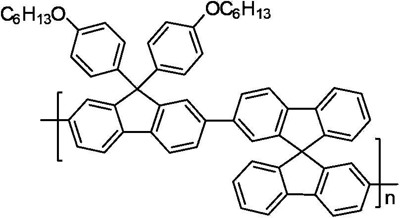
[0041] This embodiment discloses poly{2,7-diyl-9,9-bis(4-n-hexaneoxybenzene) fluorene-co-2,2'-diyl-9,9'-spiro two with the following structural formula Fluorene} (organic semiconductor material P1):

[0042]

[0043] The preparation process of the above organic semiconductor material P1 is as follows:

[0044] Under the protection of argon, 9,9-bis(4-n-hexaneoxybenzene) fluorene-2,7-dipinacol borate (154mg, 0.2mmol), 2,2'dibromo-9, 9'-Spirobifluorene (95mg, 0.2mmol) was added to the flask containing 10ml of toluene solvent, after fully dissolved, potassium carbonate (2mL, 2mol / L) solution was added to the flask, vacuumed to remove oxygen and filled with argon , Then add bistriphenylphosphine palladium dichloride (5.6mg, 0.008mmol); heat the flask to 100°C for Suzuki coupling reaction for 48h. After cooling, the polymerization reaction was stopped, and 50ml methanol was added dropwise to the flask for sedimentation; after filtering through a Soxhlet extractor, it was extracted wit...

Embodiment 2

[0053] This embodiment discloses poly{2,7-diyl-9,9-bis(4-methoxybenzene)fluorene-co-2,2'-diyl-9,9'-spirobifluorene with the following structural formula } (Organic Semiconductor Material P2):

[0054]

[0055] Under the protection of a mixture of nitrogen and argon, 9,9-bis(4-methaneoxybenzene) fluorene-2,7-dipinacol borate (189mg, 0.3mmol), 2,2'dibromo -9,9'-spirobifluorene (142mg, 0.3mmol) and 15mL of tetrahydrofuran were added to a 50mL two-necked flask. After being fully dissolved, a mixture of nitrogen and argon was introduced to exhaust the air for about 20 minutes, and then tetratriphenylene Phosphine palladium (4mg, 0.003mmol) was added to it, and after it was fully dissolved, sodium bicarbonate (3mL, 2mol / L) solution was added. After fully ventilating the mixed gas of nitrogen and argon for about 10 minutes, the two-necked flask was added to 70 ℃ for Suzuki coupling reaction for 96 hours. After cooling down, the polymerization reaction was stopped, and 40ml methanol wa...


PUM

PropertyMeasurementUnit
luminanceaaaaaaaaaa

Abstract

The present invention provides an organic semiconductor material having the following chemical formula, wherein R is C1-C20 alkyl, and n is an integer of 10-100. According to the present invention, the hole transporting property of the organic semiconductor material is 10<-5> cm<2> / (V.s) magnitude order, and the organic semiconductor material has a high triplet energy level of greater than 2.7 eV, such that the condition that energy is returned to the main body material during the luminescence process can be effectively prevented so as to substantially increase the luminescence efficiency; the organic semiconductor material can be used as the blue light phosphorescent main body material; and the organic semiconductor material preparation method adopts the simple synthesis route, and has characteristics of process reducing, easily available raw materials and manufacturing cost reducing.

Description

Technical field [0001] The invention belongs to the field of optoelectronic materials, and specifically relates to an organic semiconductor material, a preparation method and an electroluminescent device. Background technique [0002] Organic electroluminescent devices have the advantages of low driving voltage, fast response speed, wide viewing angle range, and the ability to fine-tune the chemical structure to change the luminous performance to make the color rich, easy to achieve high resolution, light weight, large-area flat panel display, etc., known as " Flat panel display technology in the 21st century" has become a hotspot in the fields of materials, information, physics and other disciplines and flat panel displays. In the future, high-efficiency commercial organic light-emitting diodes will likely contain organometallic phosphors, because they can trap both singlet and triplet excitons, thereby achieving 100% internal quantum efficiency. However, due to the relatively ...

Claims


Application Information

Patent Timeline
Patent Type & Authority Applications(China)
IPC IPC(8): C08G61/02C07C41/30C07C43/21H01L51/54
Inventor 周明杰王平张振华黄辉
Owner OCEANS KING LIGHTING SCI&TECH CO LTD
Why Eureka
Try Eureka