MEMS capacitor switch with PN junction

A technology of capacitive switch and PN junction, which is applied in the field of electronic science, can solve the problems of applying large electrostatic force, high series impedance, and the switch cannot be released, so as to improve reliability and stability, ensure close contact, and avoid bonding failure Effect

Inactive Publication Date: 2014-08-13
UNIV OF ELECTRONICS SCI & TECH OF CHINA
View PDF5 Cites 10 Cited by
  • Summary
  • Abstract
  • Description
  • Claims
  • Application Information

AI Technical Summary

Problems solved by technology

The MEMS capacitive switch with a contact pull-down structure will cause charge injection and accumulation effects in the insulating dielectric layer 4 after long-term application of a DC bias driving voltage, and finally the insulating dielectric layer 4 cannot be released due to excessive charge accumulation, that is, adhesion fail
figure 2 In the shown non-contact pull-down driving electrode structure, after a DC bias driving voltage is applied between the upper and lower driving electrodes, the upper and lower driving electrodes generate electrostatic force, and the electrostatic force pulls down the upper driving electrode 3 (ie, the pull-down driving electrode), so that The electrical contact point 2 on the cantilever beam is in contact with the signal line 7 to produce radio frequency switching characteristics, but when the electrical contact point 2 is in contact with the signal line 7, there is still a certain gap 4' between the upper and lower driving electrodes without direct contact, so as to avoid the medium The effect of layer charge injection, but because it is necessary to avoid excessive pull-down electrostatic force that makes the upper and lower electrodes directly contact and cause a DC short circuit, it is impossible to apply a large electrostatic force, which will cause the electrical contact point 2 and the signal line 7 to not be in close contact, resulting in switching The radio frequency performance is degraded (such as large insertion loss, too high series impedance introduced, etc.)

Method used


Image

  • MEMS capacitor switch with PN junction
  • MEMS capacitor switch with PN junction
  • MEMS capacitor switch with PN junction

Examples


Embodiment Construction

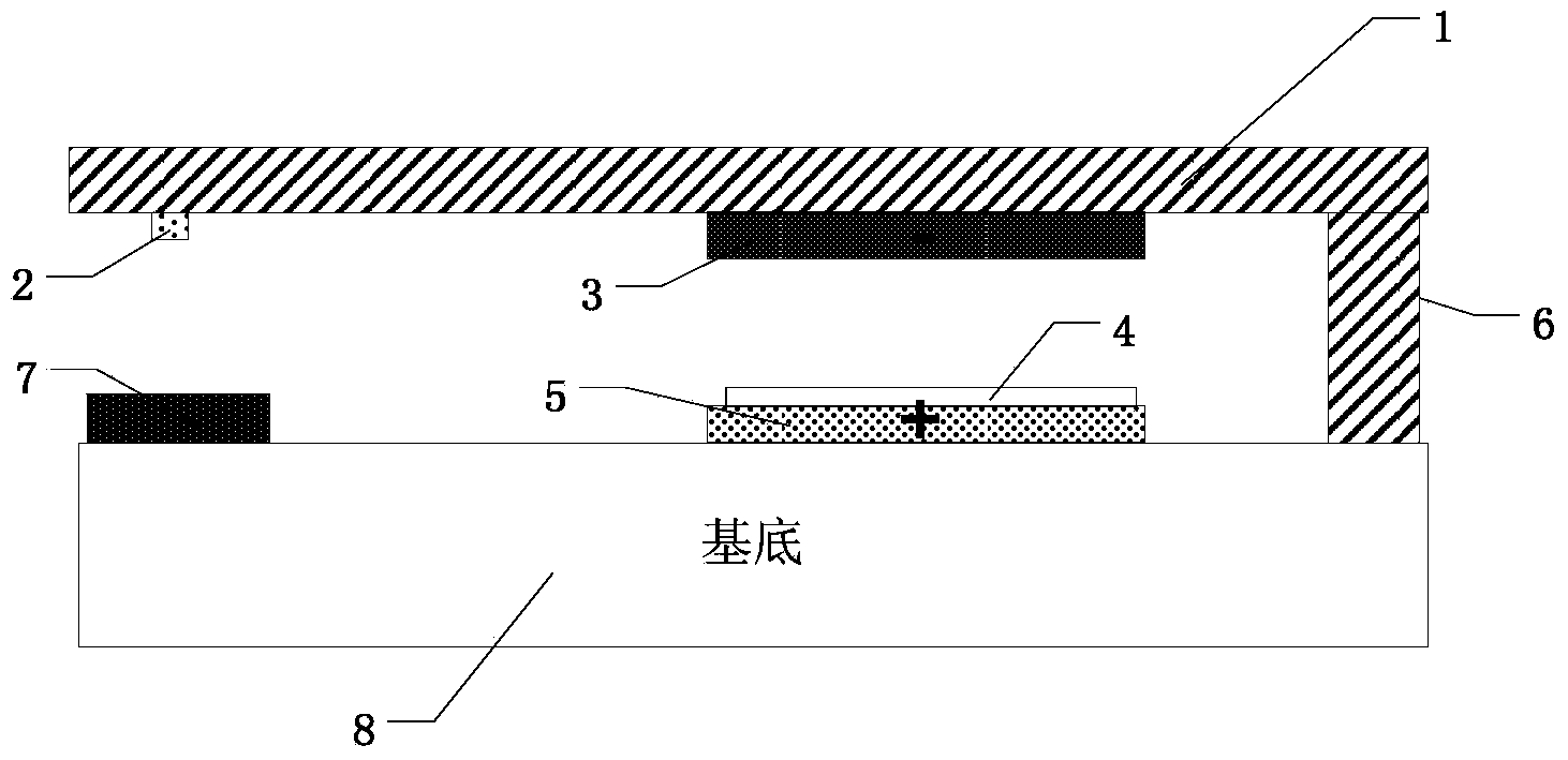
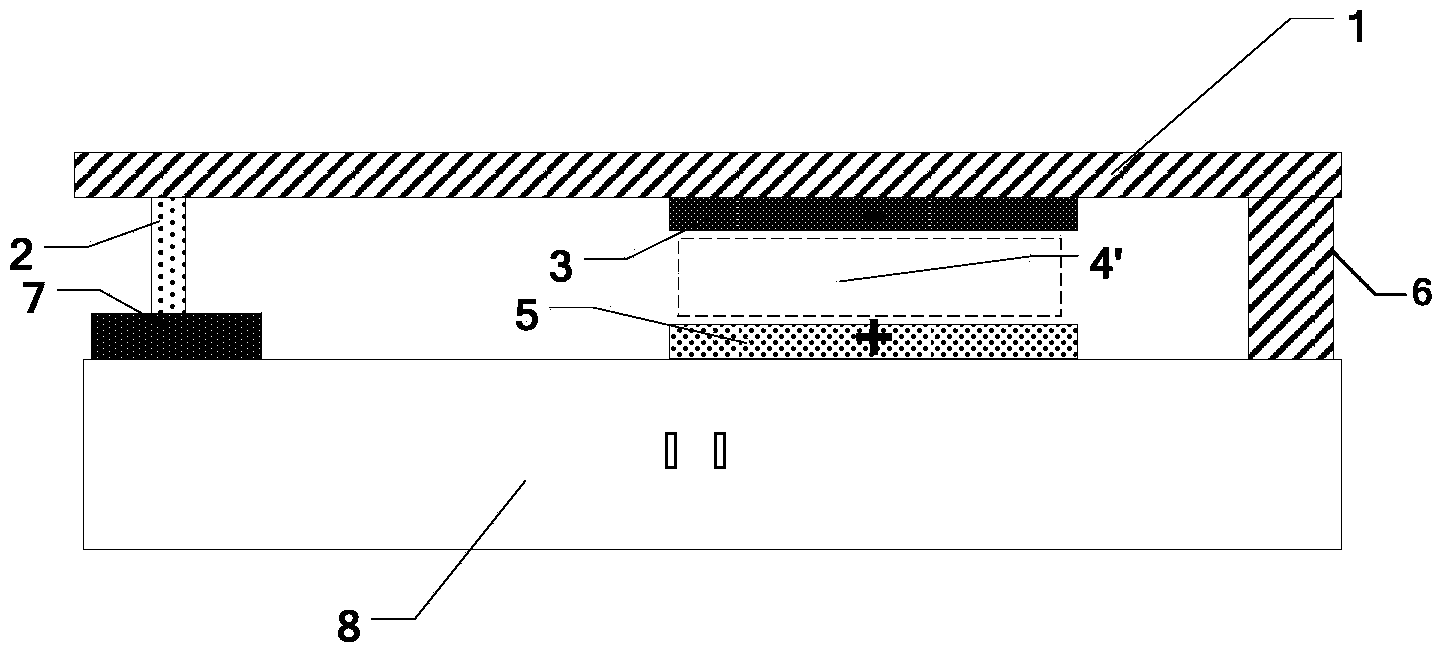
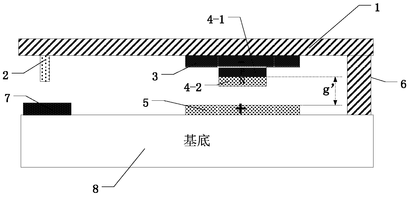
[0034] Below in conjunction with accompanying drawing, the present invention will be further described. Such as Figure 3 to Figure 5 as shown,

[0035] A MEMS capacitive switch with a PN junction, comprising a cantilever beam 1 and a signal line 7 arranged on the surface of a substrate substrate 8, one end of the cantilever beam 1 is fixed on the substrate substrate 8 by an anchor point 6, and the cantilever beam 1 The other end is provided with an electrical contact point 2 capable of connecting two sections of signal lines 7; a lower drive electrode 5 is provided on the surface area of ​​the substrate substrate 8 between the signal line 7 and the anchor point 6, correspondingly on the cantilever beam 1 The area between the anchor point 6 and the electrical contact point 2 is provided with an upper driving electrode 3, and there is a vertical semiconductor PN junction composed of a P-type semiconductor 4-1 and an N-type semiconductor 4-2 between the upper and lower driving ...


PUM


Abstract

The invention discloses an MEMS capacitor switch with a PN junction, and belongs to the technical field of electronics. The MEMS capacitor switch is characterized in that a longitudinal PN junction structure is additionally arranged between an upper drive electrode and a lower drive electrode of the MEMS capacitor switch; when the switch is in the Up state, drive voltage is not applied between the upper drive electrode and the lower drive electrode, and an electric contact point does not make contact with a signal line; when the switch is in the Down state, the upper drive electrode is pulled downwards under the action of the drive voltage, the electric contact point makes contact with the signal line, and meanwhile the longitudinal semiconductor PN junction is in the reversal of biasing state. When the MEMS capacitor switch with the PN junction works in the Down state, charge injection and accumulation cannot be generated, the bonding failure problem of the upper drive electrode and the lower drive electrode is solved, the MEMS capacitor switch is made to work under the sufficient drive voltage, it can be guaranteed that the electric contact point tightly makes contact with the signal line, and eventually reliability and stability of the MEMS capacitor switch can be improved.

Description

technical field [0001] The invention belongs to the field of electronic science and technology, relates to microelectromechanical systems (MEMS) and semiconductor technology, and specifically refers to a MEMS capacitance switch with a PN junction. technical background [0002] Switches are fundamental components in radio frequency (RF) and microwave communication systems, and radio frequency microelectromechanical (RF MEMS) switches have great application space at both the RF and microwave component and system levels. At the component level, radio frequency microelectromechanical (RF MEMS) switches can be used to construct voltage-controlled oscillators, filters (capacitive switches, inductors) and phase shifters, etc., which are indispensable components of modern radar and communication systems. Compared with traditional FET and PIN diode switches, radio frequency microelectromechanical (RF MEMS) switches have the characteristics of low DC power consumption, low insertion l...

Claims


Application Information

Patent Timeline
Patent Type & Authority Applications(China)
IPC IPC(8): H01H59/00H01L29/06
Inventor 鲍景富李昕熠黄裕霖李立圆黄洪云
Owner UNIV OF ELECTRONICS SCI & TECH OF CHINA
Why Eureka
Try Eureka