Backside illuminated low-crosstalk image sensor pixel structure and manufacturing method thereof
An image sensor and pixel structure technology, applied in radiation control devices, etc., can solve problems such as image distortion, achieve the effects of curbing crosstalk, improving photosensitivity, and avoiding crosstalk
- Summary
- Abstract
- Description
- Claims
- Application Information
AI Technical Summary
Problems solved by technology
Method used
Image

Examples
Embodiment 1
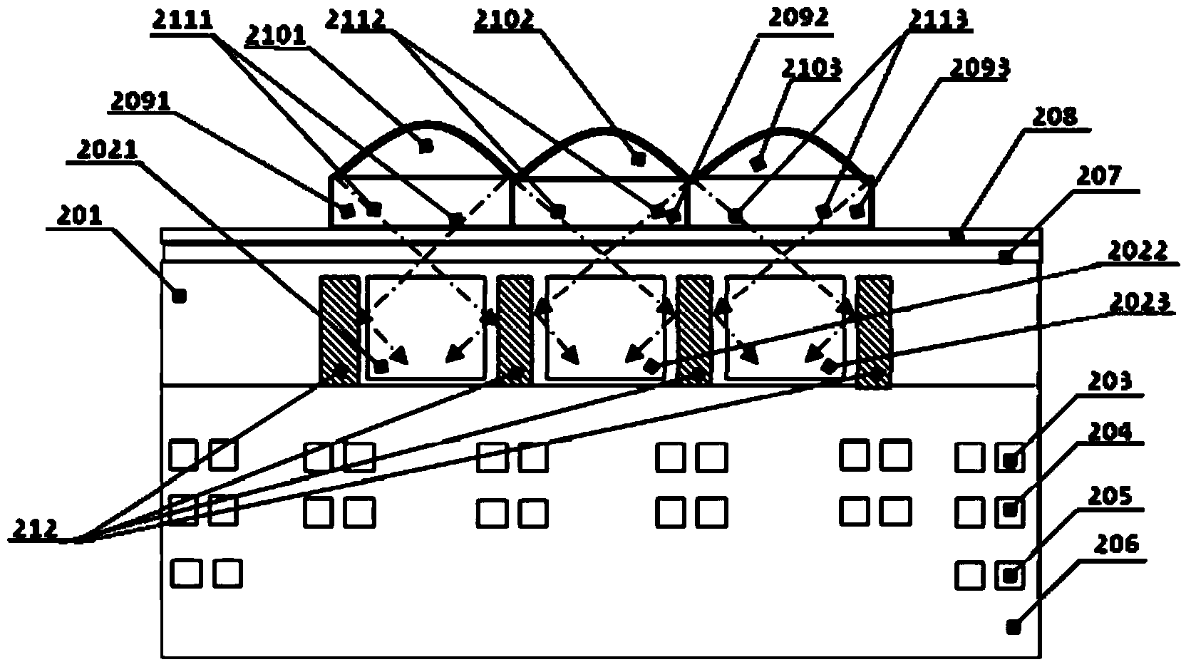
[0049] like figure 2 As shown, the pixel structure of the back-illuminated low crosstalk image sensor in this embodiment includes: a silicon substrate 201, three adjacent photosensitive devices 2021-2023, front metal interconnect lines 203-205, and a front metal interconnect line dielectric layer 206, backside anti-reflection coating 207, backside flat layer 208, backside color filters 2091-2093, backside microlenses 2101-2103, anti-crosstalk layer 212, and at the same time figure 2 A set of incident rays 2111-2113 is given. Among them, the anti-crosstalk layer 212 is located between the adjacent photosensitive devices 2021, 2022, 2023, and its depth is 2-4um, and the coverage is from the front surface of the silicon substrate to the back surface of the silicon substrate 0.05um-0.2um, which is much larger than the traditional The depth of the integrated circuit shallow trench isolation trench is 0.3 to 0.5um. The anti-crosstalk layer 212 uses an ion implantation process to...
Embodiment 2
[0051] In order to further clearly illustrate the features of the present invention, Figure 3 to Figure 8 One of the manufacturing process flow of the back-illuminated image sensor pixel of the present invention is characterized in detail.
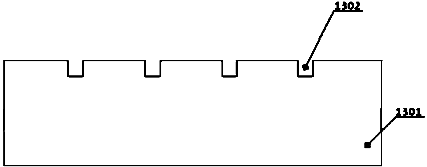
[0052] image 3 Shown is a substrate 1301 for making a back-illuminated image sensor. According to traditional integrated circuits, a shallow trench isolation trench (STI) 1302 for isolating devices is formed after photolithography, etching and other process steps, and its depth is about 0.3um -0.5um.
[0053] Figure 4 shown is based on image 3 In the further fabrication process, the STI 1402 is formed on the substrate 1401 and the photoresist 1403 is further coated in the STI area. After exposure and development, the photoresist on the STI is removed to form an opening area of 1404, and the oxygen is further removed by ion implantation. Ions 1405 are implanted into the substrate 1401 to form a silicon dioxide isolation layer 1406, ...
Embodiment 3
[0059] In order to further clearly illustrate the features of the present invention, Figure 9 to Figure 11 Another manufacturing process flow of the pixel of the backside illuminated image sensor of the present invention is described in detail.
[0060] Figure 9 Shown is a schematic diagram of a back-illuminated image sensor fabricated according to a conventional integrated circuit manufacturing process to the substrate 2301 after thinning.
[0061] Figure 10 shown is based on Figure 9 The further manufacturing process of the STI is firstly to uniformly coat the photoresist 2409 on the surface of the thinned substrate 2401, further, remove the photoresist on the STI by photolithography, developing and other processes, and further, adopt the injection process to inject a certain amount of energy and a certain dose of oxygen ions are implanted into the substrate 2401 to form an anti-crosstalk layer 2402 . Further, the carrier silicon 2408 is removed to form a figure 2 ...
PUM
 Abstract
Description
Claims
Application Information
 - Generate Ideas
- Intellectual Property
- Life Sciences
- Materials
- Tech Scout
- Unparalleled Data Quality
- Higher Quality Content
- 60% Fewer Hallucinations
Browse by: Latest US Patents, China's latest patents, Technical Efficacy Thesaurus, Application Domain, Technology Topic, Popular Technical Reports.
© 2025 PatSnap. All rights reserved.Legal|Privacy policy|Modern Slavery Act Transparency Statement|Sitemap|About US| Contact US: help@patsnap.com