
Transparent graphene conducting film and method for manufacturing same

A technology of transparent conductive film and transparent conductive layer, which is applied in the direction of cable/conductor manufacturing, conductive layer on insulating carrier, circuit, etc., can solve problems such as high manufacturing cost, cracks, and brittle ITO film, and achieve yield and Cost advantage, the effect of reducing manufacturing costs

Inactive Publication Date: 2014-08-20
ZHENGZHOU JUSHUNJIA ELECTRONICS TECH
View PDF4 Cites 1 Cited by
  • Summary
  • Abstract
  • Description
  • Claims
  • Application Information

AI Technical Summary

Problems solved by technology

In recent years, with the continuous development of information technology and products, the market demand for transparent conductive films is increasing. Although the ITO films produced by existing processes have high conductivity and high transparency, they can basically meet the requirements of most electronic products. The requirements of the two indicators, but there are still many insurmountable defects in the ITO film: 1. The ITO film is very brittle and fragile, and it is easy to be worn during application or cracks or fall off when it is bent, which affects the service life; 2. After the ITO film is formed High temperature treatment is required to achieve high conductivity, which limits the use of many substrates; 3. Since the main component of ITO is indium, the storage capacity is limited (the current global annual output is only about 500 tons), and the film-forming process of ITO is also limited. High-quality ITO targets must be used, and the production technology of high-quality ITO targets is mainly controlled in Japan, Europe and the United States and other countries, so affected by raw materials, production equipment and processes, ITO materials will become more and more expensive
Depositing a transparent conductive oxide film layer on the graphene transparent conductive layer is not only difficult in process and high in manufacturing cost, but also violates the conductive principle of graphene: the increased transparent conductive oxide film layer will reduce the transmission of the transparent conductive film layer. Rate
Moreover, due to the extremely fragile mechanical properties of single-layer graphene, graphene is easily damaged during the process of depositing transparent conductive oxide layers, resulting in a decrease in the electrical conductivity of graphene, which is even higher than that of the original graphene.

Method used


Image

  • Transparent graphene conducting film and method for manufacturing same

Examples


Embodiment Construction

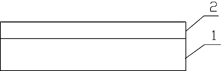
[0021] Such as figure 1 As shown, the graphene transparent conductive film of the present invention includes a substrate 1 and a graphene transparent conductive layer 2 attached to the substrate 1. The graphene transparent conductive layer 2 has a thickness of 0.3 to 1.5 nm; the thickness of the substrate 1 is 10~1000μm.

[0022] Under normal circumstances, the graphene transparent conductive layer 2 has 1 to 5 layers, and its visible light transmittance is ≥85%; preferably, the graphene transparent conductive layer 2 has 2 to 3 layers.

[0023] The substrate 1 includes glass, PET, and acrylic.

[0024] The preparation method of the graphene transparent conductive film of the present invention includes the following steps:

[0025] The first step is to prepare graphene (100um thick copper foil is used for the substrate, and methane is used for the carbon source gas)

[0026] 1. Wipe the surface of the copper foil clean with alcohol and put it into the plasma equipment for cleaning to ...


PUM

PropertyMeasurementUnit
thicknessaaaaaaaaaa
thicknessaaaaaaaaaa
transmittivityaaaaaaaaaa

Abstract

The invention discloses a transparent graphene conducting film. The transparent graphene conducting film comprises a substrate and a transparent graphene conducting layer adhering to the substrate. The thickness of the transparent graphene conducting layer ranges from 0.3 nm to 1.5 nm. The thickness of the substrate ranges from 10 microns to 100 microns. A method for manufacturing the transparent graphene conducting film comprises the following steps that firstly, a graphene thin film is manufactured, and then through transferring, the transparent graphene conducting film composed of the substrate and the transparent graphene conducting layer adhering to the substrate can be obtained. The transparent graphene conducting film and the method for manufacturing the transparent graphene conducting film have the advantages that no transparent conducting oxide film layer needs to be deposited on the graphene thin film, manufacturing cost of the transparent graphene conducting film is reduced, the transparent graphene conducting film and the method for manufacturing the transparent graphene conducting film have more advantages in rate of finishes products and cost, and due to the fact that the transparent graphene conducting film is foldable, the transparent graphene conducting film can be applied to related industries such as touch screens, liquid crystal displays and solar energy because the transparent graphene conducting film can be folded.

Description

Technical field [0001] The invention relates to a conductive film, in particular to a graphene transparent conductive film that can replace the ITO conductive film, and also relates to a method for preparing the conductive film. Background technique [0002] Transparent conductive film is a necessary raw material for the production of liquid crystal displays, OLED displays, thin-film solar cells, touch screens, electromagnetic shielding and other products. It must have the following properties: 1. The average transmittance of visible light (wavelength in the range of 380~760mm) is up to Above 80%; 2. High electrical conductivity, and square resistance below 900Ω / □. The traditionally used transparent conductive film is represented by Indium Tin Oxides (ITO), which has the most extensive research and application and is mature. It is produced by plating a composite of indium oxide and tin oxide on a substrate. It is generally industrial Use PVD (Physical Vapor Deposition) to plate ...

Claims


Application Information

Patent Timeline
Patent Type & Authority Applications(China)
IPC IPC(8): H01B5/14H01B13/00
Inventor 黄涛赵勇余洲
Owner ZHENGZHOU JUSHUNJIA ELECTRONICS TECH
Features
  • Generate Ideas
  • Intellectual Property
  • Life Sciences
  • Materials
  • Tech Scout
  • Unparalleled Data Quality
  • Higher Quality Content
  • 60% Fewer Hallucinations
Learn More