

Manufacturing method of multi-phase low dielectric constant material layer
A technology of low dielectric constant materials and manufacturing methods, applied in the manufacture of semiconductor/solid state devices, circuits, electrical components, etc., can solve problems such as poor mechanical strength, and achieve high molding strength. Effect
- Summary
- Abstract
- Description
- Claims
- Application Information
AI Technical Summary
Problems solved by technology
Method used
Image

Examples
Embodiment
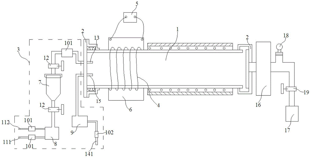
[0030] Embodiment: a kind of manufacturing method of multi-phase low dielectric constant material layer, comprises the following steps:
[0031] Step 1. Evaporating a layer of aluminum film with a thickness of 80 nm on the silicon substrate by electron beam evaporation under vacuum conditions;
[0032] Step 2, then vapor-deposit a layer of nickel film with a thickness of 5nm to form a silicon wafer with a metal film under the condition of not breaking the vacuum;
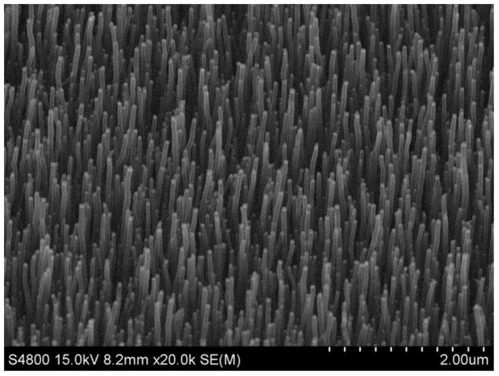
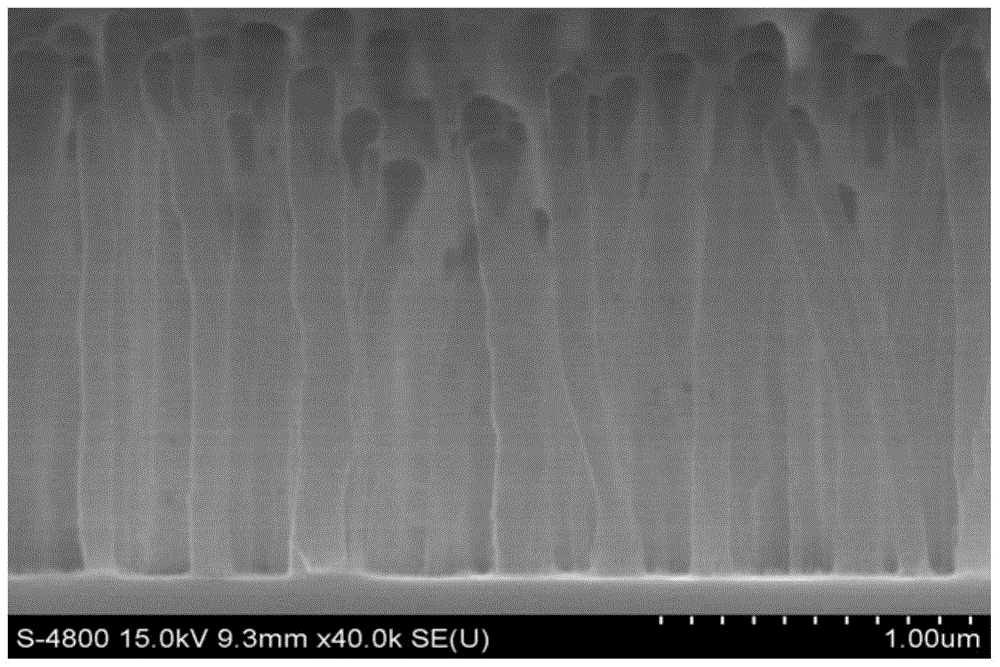
[0033] Step 3: Anneal the metal thin film in step 2 at 600°C under the protection of ammonia gas flow for 3 minutes, then raise the temperature to 750°C, and feed in a mixture of ammonia and acetylene with a ratio of 4:1. Gas, the reaction time of this step is 15 minutes, the vacuum degree in the chamber is 7Torr, the plasma power is 210W, and the applied voltage is 530V, so that a layer of carbon is deposited on the silicon wafer of the metal film by the plasma enhanced chemical vapor deposition method. The nanotu...
PUM
 Abstract
Description
Claims
Application Information