GaN-based light-emitting diode structure and preparation method thereof

A technology of light-emitting diodes and light-emitting layers, which is applied to electrical components, circuits, semiconductor devices, etc., and can solve the problems of severe light absorption of p-type gallium nitride layers, low concentration of Mg-doped hole carriers, and difficulties in p-type doping, etc. question

Inactive Publication Date: 2014-09-03
SHANDONG INSPUR HUAGUANG OPTOELECTRONICS
View PDF6 Cites 6 Cited by
  • Summary
  • Abstract
  • Description
  • Claims
  • Application Information

AI Technical Summary

Problems solved by technology

[0009] Aiming at the problems of low Mg-doped hole carrier concentration, difficult p-type doping and serious light absorption of p-type gal

Method used


Image

  • GaN-based light-emitting diode structure and preparation method thereof
  • GaN-based light-emitting diode structure and preparation method thereof

Examples


Embodiment 1

[0043] Embodiment 1. Preparation of a GaN-based light-emitting diode with the same-plane electrode structure on a sapphire substrate.

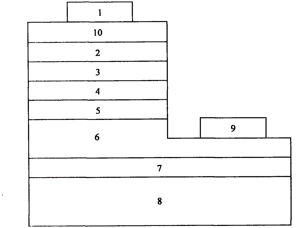
[0044] Such as figure 1 As shown, the GaN-based light-emitting diode structure with the same-plane electrode structure is sequentially sapphire substrate 8, buffer layer 7, n-type GaN conductive layer 6, n-type AlGaN confinement layer 5, active region light-emitting layer 4, A p-type AlGaN confinement layer 3, a p-type diamond thin film conductive layer 2, an ITO transparent conductive layer 10 and a p electrode 1; an n electrode 9 is prepared on an n-type GaN conductive layer 6; the p-type diamond thin film conductive layer 2 is grown On the upper surface of the p-type AlGaN confinement layer 3 , the thickness is 50 nm; the cross-sectional size of the p-type diamond thin film conductive layer 2 is the same as that of the p-type AlGaN confinement layer 3 .

[0045] The preparation method steps are as follows:

[0046] (1) Prepare the epitaxi...

Embodiment 2

[0049] Embodiment 2. Preparation of a GaN-based light-emitting diode with a vertical electrode structure on a silicon carbide substrate.

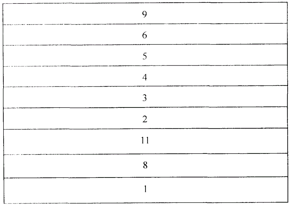
[0050] Such as figure 2 As shown, the vertical electrode structure GaN-based light-emitting diode structure sequentially includes a p-electrode 1, a silicon carbide substrate 8, a p-type ohmic contact layer 11, a p-type diamond thin film conductive layer 2, and a p-type AlGaN confinement layer 3 from bottom to top. , an active region light-emitting layer 4, an n-type AlGaN confinement layer 5, an n-type GaN conductive layer 6 and an n-electrode 9; the p-type diamond film conductive layer 2 is grown on the lower surface of the p-type AlGaN confinement layer 3, with a thickness of 500 nm; the cross-sectional size of the p-type diamond thin film conductive layer 2 is the same as the size of the p-type AlGaN confinement layer 3 .

[0051] The preparation method steps are as follows:

[0052] (1) Prepare the epitaxial wafer to the p-type AlGa...

Embodiment 3

[0055] Embodiment 3. GaN-based light-emitting diodes with the same-plane electrode structure prepared on a silicon substrate.

[0056] Such as figure 1 As shown, as shown in Embodiment 1, the GaN-based light-emitting diode structure sequentially includes a silicon substrate 8, a buffer layer 7, an n-type GaN conductive layer 6, an n-type AlGaN confinement layer 5, and an active region light-emitting layer from bottom to top. 4. P-type AlGaN confinement layer 3, p-type diamond film conductive layer 2, ITO transparent conductive layer 10 and p-electrode 1; the preparation method is as described in Example 1, the difference is:

[0057] The chemical vapor deposition method described in step (1) is a combustion flame chemical vapor deposition method; the thickness of the p-type diamond film conductive layer 2 is 200nm; the temperature condition is 700 degrees Celsius, and the growth time is 30 minutes; the methane, The volume ratio of hydrogen and borane is 1:85:0.002; the doping...


PUM

PropertyMeasurementUnit
Thicknessaaaaaaaaaa
Thicknessaaaaaaaaaa
Thicknessaaaaaaaaaa

Abstract

The invention relates to a GaN-based light-emitting diode structure which comprises a substrate, an n-type GaN conductive layer, an n-type AlGaN limitation layer, an active region luminous layer, a p-type AlGaN limitation layer, a p electrode and an n electrode. A layer of p-type diamond film conductive layer is deposited on the upper surface or the lower surface of the p-type AlGaN limitation layer. The size of the cross sectional area of the p-type diamond film conductive layer is the same with the size of the p-type AlGaN limitation layer, and the thickness of the p-type diamond film conductive layer is 50-500 nm. The diamond film has a weak absorption effect on full-waveband light, so that light absorption is reduced, and light extraction efficiency of LED can be effectively improved; the forbidden band width of diamond is relatively large, so that the reflection effect on electrons is strong, electron leakage can be reduced, and brightness is improved; and the p-type diamond film is easy to dope, the hole concentration is relatively high, and ohmic contact is easy to prepare.

Description

technical field [0001] The invention relates to a GaN-based light-emitting diode structure and a preparation method thereof, belonging to the technical field of semiconductors. Background technique [0002] Light-emitting diode (referred to as "LED") is a semiconductor solid-state light-emitting device, which uses the conduction band electrons and valence band holes inside the semiconductor material to undergo radiative recombination, and releases energy in the form of photons to directly emit light. By designing different bandgap widths of semiconductor materials, light-emitting diodes can emit light in different bands from infrared to ultraviolet. [0003] Nitride light-emitting diodes have been widely developed around the world due to their advantages of high efficiency, energy saving, long life and small size. Ultraviolet light-emitting diodes with a luminous wavelength of 210-365nm have broad application prospects in the fields of sterilization, biomedicine, lighting, ...

Claims


Application Information

Patent Timeline
IPC IPC(8): H01L33/40H01L33/02H01L33/00
CPCH01L33/007H01L33/40
Inventor 王成新徐明升曲爽马旺徐现刚
Owner SHANDONG INSPUR HUAGUANG OPTOELECTRONICS
Why Eureka
Try Eureka