Thermally enhanced wiring board with built-in heat sink and build-up circuitry

A heat sink, gain-type technology, applied in circuit thermal devices, circuits, printed circuits, etc., can solve problems such as limiting routing feasibility, reducing heat dissipation, and limiting heat dissipation, so as to be suitable for mass manufacturing and prevent thermal connection. The effect of false, high routing feasibility

Inactive Publication Date: 2014-09-10
BRIDGE SEMICON
View PDF10 Cites 10 Cited by
  • Summary
  • Abstract
  • Description
  • Claims
  • Application Information

AI Technical Summary

Problems solved by technology

For example, dielectric layers with low thermal conductivity, such as epoxy resins, limit heat dissipation; however, interposed heat sinks may warp during manufacturing due to heat, or undergo early debonding, or during operation. An error occurred
Lead frame type substrates may limit routing feasibility, or multilayer circuits with thick dielectric layers may reduce heat dissipation
Heat sinks may fail, respond slowly, or have difficulty thermally connecting to the next level of assembly
Its manufacturing process may not be suitable for low-cost and high-volume manufacturing

Method used


Image

  • Thermally enhanced wiring board with built-in heat sink and build-up circuitry
  • Thermally enhanced wiring board with built-in heat sink and build-up circuitry
  • Thermally enhanced wiring board with built-in heat sink and build-up circuitry

Examples


Embodiment 1

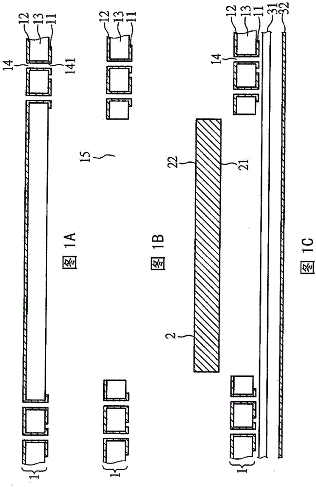
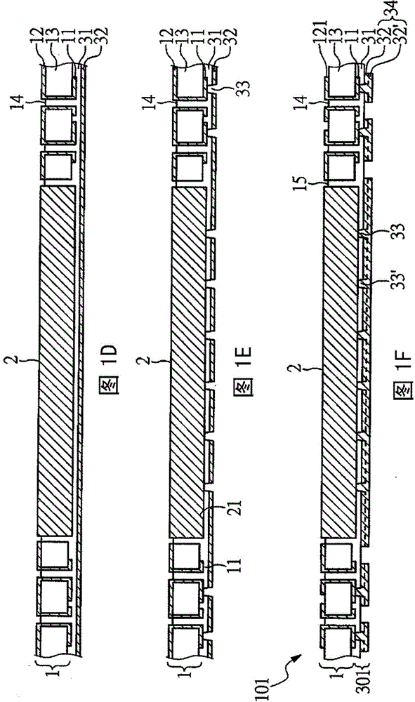
[0039] Figure 1A — 1F is a cross-sectional view of a method for manufacturing a thermally enhanced circuit board according to a preferred embodiment of the present invention. The circuit board includes a reinforcement layer, a heat sink, and a build-up circuit electrically connected to the reinforcement layer.

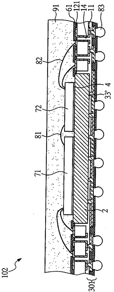
[0040] Such as Figure 1F As shown, the thermally enhanced circuit board 101 includes a reinforcement layer 1 , a heat sink 2 , and a build-up circuit 301 . The reinforcement layer 1 includes a first patterned circuit layer 11 , covered through holes 14 , a second patterned circuit layer 121 opposite to the first patterned circuit layer 11 and electrically connected to the first patterned circuit layer 11 , and via holes 15 , which is put into heat sink 2. The build-up circuit 301 includes a first dielectric layer 31 , a first blind hole 33 , and a first wire 34 . The build-up circuit 301 is respectively thermally connected to the heat sink 2 and electrically conne...

Embodiment 2

[0052] For the purpose of brevity, any statement in Example 1 may be incorporated into the same application section here, and the same statement will not be repeated.

[0053] Figure 2A and 2B is a cross-sectional view of a method for forming the positioning member 17 on the first dielectric layer 31 according to another preferred embodiment of the present invention; and Figure 2C for correspondence Figure 2B top view.

[0054] Figure 2A It is a structural cross-sectional view of a laminated substrate having a metal layer 16 , a first dielectric layer 31 and a support plate 35 . The metal layer 16 is shown as a copper layer with a thickness of 35 μm, however, the metal layer 16 can also be made of other various metal materials and is not limited to the copper layer. In addition, the metal layer 16 can be deposited on the first dielectric layer 31 in a single-layer or multi-layer structure by various techniques such as pressing, electroplating, electroless plating, eva...

Embodiment 3

[0074] Figure 4A-Figure 4DIt is a cross-sectional view of another circuit board manufacturing method according to another preferred embodiment of the present invention. The circuit board includes a heat sink, a positioning member, a reinforcing layer, and a double build-up circuit.

[0075] For the purpose of brevity, any statement in Example 1 may be incorporated into the same application section here, and the same statement will not be repeated.

[0076] Please refer to Figure 3A and Figure 3B The structure, after using the adhesive 4 and using the positioning piece 17 as a configuration guide, the heat sink 2 is arranged on the first dielectric layer 31, the positioning piece 17 and the heat sink 2 are aligned with the through hole 15 of the reinforcement layer 1 and extending into it, and using an adhesive 4 to place the reinforcement layer 1 on the first dielectric layer 31 . Such as Figure 4A As shown, the heat sink 2 and the through hole 15 of the reinforcing la...


PUM


Abstract

A thermally enhanced wiring board includes a heat sink, a stiffener and a build-up circuitry. The heat sink extends into an aperture of the stiffener and is thermally connected to the build-up circuitry. The build-up circuitry covers the heat sink and the stiffener and provides signal routing for the stiffener. The stiffener provides signal routing and mechanical support for the build-up circuitry.

Description

technical field [0001] The invention relates to a circuit board, in particular to a heat dissipation gain type circuit board with a built-in heat sink, a strengthening layer, and a layer-up circuit for a semiconductor assembly. Background technique [0002] Semiconductor components have high voltage, high frequency, and high performance applications that require high power to perform the specific functions. Semiconductor components generate more heat due to increased power. For portable electronic devices, their high packaging density and small size reduce the surface area for heat dissipation, which may make heat accumulation more serious. [0003] Semiconductor components are prone to performance degradation, short lifetime and immediate errors at high operating temperatures. Thermal energy not only degrades the chip, but also puts thermal stress on the chip and surrounding components due to thermal expansion mismatch. Therefore, the chip must be assembled to the heat s...

Claims


Application Information

Patent Timeline
Patent Type & Authority Applications(China)
IPC IPC(8): H05K1/02H01L23/498H01L23/367
CPCH01L2924/0002H01L2924/15311H01L2224/48137H01L2224/48091H01L2224/73265H05K1/0271H01L2224/48227H01L2224/32225H01L2224/45144H05K1/0206H05K3/3436H05K3/4652H05K3/4697H05K2201/10416H01L2924/181H01L2224/32245H01L2924/00014H01L2924/00H01L2924/00012
Inventor 林文强王家忠
Owner BRIDGE SEMICON
Why Eureka
Try Eureka