Avalanche photo diode detector systems

A diode detector, avalanche photoelectric technology, applied in the direction of using electric radiation detectors for photometry, electrical components, measurement circuits, etc., can solve the problem of increased bit error rate and other issues

Active Publication Date: 2014-09-17
MAXIM INTEGRATED PROD INC
View PDF10 Cites 6 Cited by
  • Summary
  • Abstract
  • Description
  • Claims
  • Application Information

AI Technical Summary

Problems solved by technology

The variability of the M factor can lead to a significa

Method used


Image

  • Avalanche photo diode detector systems
  • Avalanche photo diode detector systems
  • Avalanche photo diode detector systems

Examples


Embodiment Construction

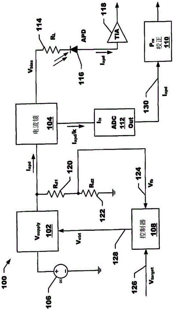
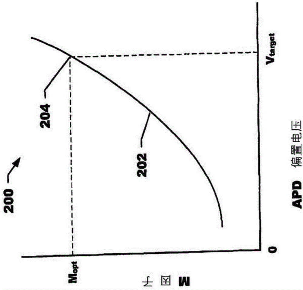
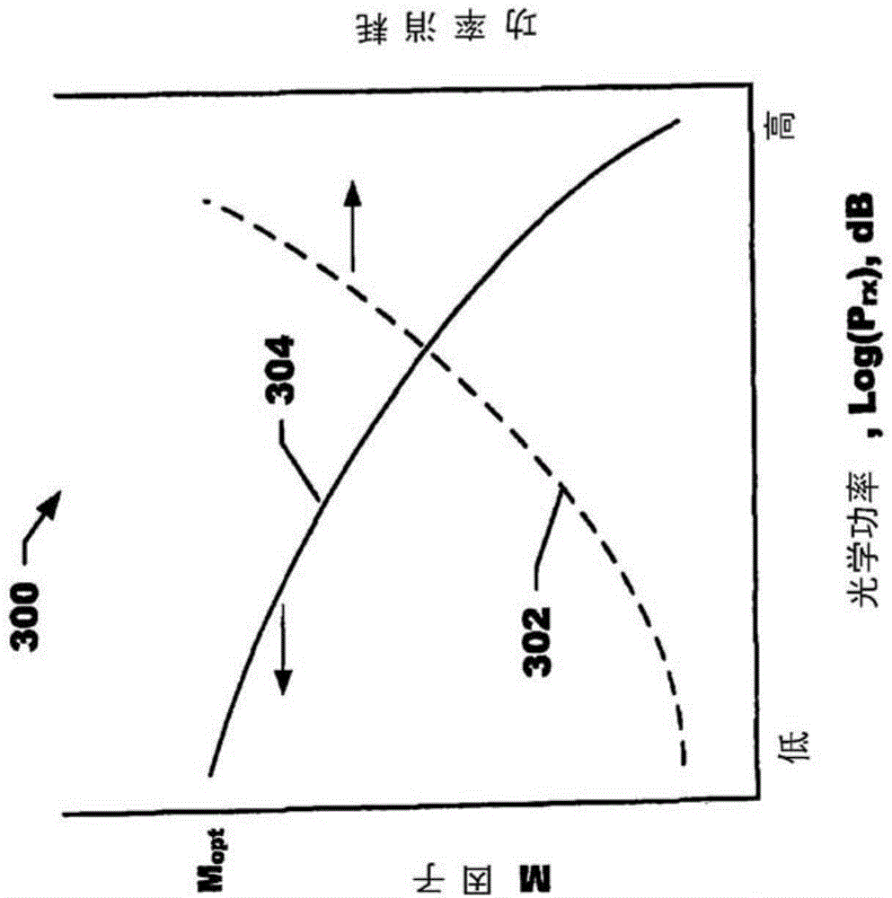
[0022] discussed with reference to prior art Figure 1-3 . Figure 4 is a graph 400 of the multiplication factor M as a function of APD bias voltage for an example control system embodiment. Plot 402 illustrates the variation of the M factor with applied bias voltage for the APD. A point 404 on the plot 402 is selected to yield the most desired working M factor M opt The high voltage (V H ) working point. This M factor is chosen for operation at the lowest suitable input optical power level and gives a sufficient output data signal level. For high input power levels at M min , plot 402 on corresponds to lower bias voltage V LAt point 406, under Work, select the second M factor. A lower M factor M was chosen for several considerations min . At high input optical power levels, the APD will generate large currents due to the higher illumination levels, and does not require a large M factor to generate sufficiently high output signal levels. In fact, operating the APD wi...


PUM


Abstract

An avalanche photo diode detector including an avalanche photo diode, an adjustable voltage source, a current mirror coupled to the voltage source output of the adjustable voltage source and having a current measurement output, and a processor coupled to the adjustable voltage source and the current mirror. The processor implements a process of obtaining a signal current measurement from the current mirror, computing an estimate of an input optical power level from the signal current measurement and adjusting the output of the adjustable voltage source based upon on the estimate of the input optical power level.

Description

Background technique [0001] Avalanche photodiode detectors (APDs) are utilized in a wide range of applications including low-level light detection, laser range finders, LIDAR, photon counting, optical tomography, fluorescence detection, particle screening and counting, and communication systems. APDs are particularly useful in fiber optic-based network communication systems, in particular long-reach / high-sensitivity optical receivers. [0002] Typically, during operation, the ADP is reverse biased by a relatively high voltage. When illuminated with photons of the appropriate wavelength, the diode undergoes an avalanche breakdown that creates a large signal current. The ratio between the current flowing in the absence of illumination (“dark” current) and the signal current flowing during photon-induced avalanche breakdown is the APD gain, typically referred to as a dimensionless constant called the multiplication factor (M) . [0003] figure 1 is a circuit diagram of a typi...

Claims


Application Information

Patent Timeline
IPC IPC(8): G01R31/26
CPCG01J1/44H03G3/3084
Inventor J·C·阮J·菲利普
Owner MAXIM INTEGRATED PROD INC
Why Eureka
Try Eureka