Low-temperature poly-silicon manufacturing method, method for manufacturing TFT substrate by utilization of low-temperature poly-silicon manufacturing method, and TFT substrate structure

A technology of low-temperature polysilicon and a manufacturing method, which is applied to the manufacturing method and structure of TFT substrate, and the manufacturing field of low-temperature polysilicon, can solve the problems of very strict requirements on mask precision and difficulty in mass production, so as to improve display effect and reduce crystallinity. The number of bounds, the effect of the simple method

Inactive Publication Date: 2014-09-24
TCL CHINA STAR OPTOELECTRONICS TECH CO LTD
View PDF4 Cites 29 Cited by
  • Summary
  • Abstract
  • Description
  • Claims
  • Application Information

AI Technical Summary

Problems solved by technology

However, these methods require additional technologies and processes, and have very strict requirements on the accuracy of the mask, resulting in difficulties in mass production.

Method used


Image

  • Low-temperature poly-silicon manufacturing method, method for manufacturing TFT substrate by utilization of low-temperature poly-silicon manufacturing method, and TFT substrate structure
  • Low-temperature poly-silicon manufacturing method, method for manufacturing TFT substrate by utilization of low-temperature poly-silicon manufacturing method, and TFT substrate structure
  • Low-temperature poly-silicon manufacturing method, method for manufacturing TFT substrate by utilization of low-temperature poly-silicon manufacturing method, and TFT substrate structure

Examples


Embodiment Construction

[0054] In order to further illustrate the technical means adopted by the present invention and its effects, the following describes in detail in conjunction with preferred embodiments of the present invention and accompanying drawings.

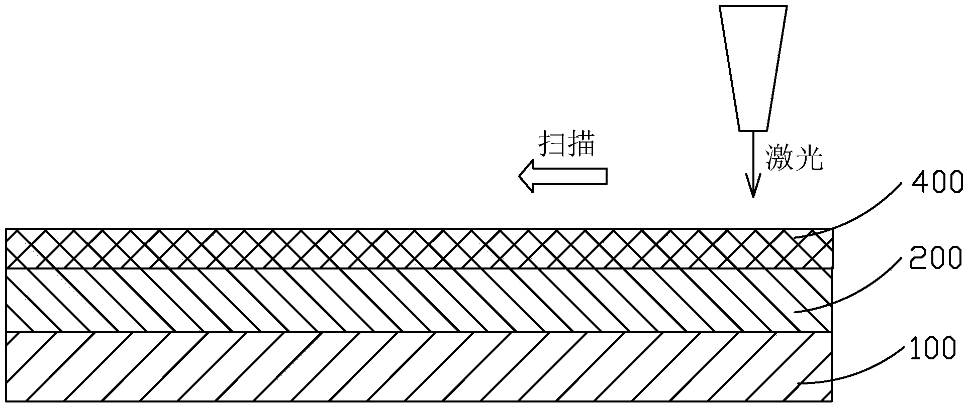
[0055] see Figure 6 and Figure 8 to Figure 13 , the invention provides a method for manufacturing low-temperature polysilicon, comprising the steps of:

[0056] Step 1, providing a substrate 1 .

[0057] The substrate 1 is a transparent substrate, preferably, the substrate 1 is a glass substrate.

[0058] Step 2, depositing and forming a buffer layer 2 on the substrate 1 .

[0059] Such as Figure 8 As shown, the thickness of the buffer layer 2 deposited and formed in step 2 is uniform. The buffer layer 2 is made of SiNx, SiOx, or a combination of SiNx and SiOx.

[0060] Step 3, patterning the buffer layer 2 to form protrusions 21 and depressions 23 with different thicknesses.

[0061] Such as Figure 9 , Figure 10 As shown, there ...


PUM


Abstract

The invention provides a low-temperature poly-silicon manufacturing method, a method for manufacturing a TFT substrate by utilization of the low-temperature poly-silicon manufacturing method, and a TFT substrate structure. The low-temperature poly-silicon manufacturing method comprises the following steps that 1, the substrate (1) is provided; 2, a buffer layer (2) is formed on the substrate (1) in a deposition mode; 3, pattern processing is carried out on the buffer layer (2), and a convex portion (21) and a concave portion (23) which are different in thickness are formed; 4, an amorphous silicon layer (3) is formed on the buffer layer (2) provided with the convex portion (21) and the concave portion (23) in a deposition mode; 5, excimer laser annealing pretreatment is carried out on the amorphous silicon layer (3); 6, excimer laser annealing is carried out on the amorphous silicon layer (3), the whole surface of the amorphous silicon layer (3) is scanned through laser beams, and the amorphous silicon layer (3) is made to melt and is recrystallized to form a poly-silicon layer (4). The method can effectively control the crystallization position and crystallization direction when the amorphous silicon layer is recrystallized.

Description

technical field [0001] The invention relates to the field of display technology, in particular to a method for manufacturing low-temperature polysilicon, a method for manufacturing a TFT substrate using the method, and a structure of the TFT substrate. Background technique [0002] With the development of flat panel displays, the demand for panels with high resolution and low energy consumption is constantly being raised. Due to its high electron mobility, Low Temperature Poly-Silicon (LTPS) has attracted the attention of the industry in the technology of Liquid Crystal Display (LCD) and Organic Light Emitting Diode (OLED) , is regarded as an important material to realize low-cost full-color flat panel display. For flat panel displays, the use of low-temperature polysilicon materials has the advantages of high resolution, fast response, high brightness, high aperture ratio, and low energy consumption, and low-temperature polysilicon can be produced at low temperatures and c...

Claims


Application Information

Patent Timeline
Patent Type & Authority Applications(China)
IPC IPC(8): H01L21/268B23K26/00H01L27/12H01L29/786H01L21/77
CPCH01L21/02422H01L21/02488H01L21/02513H01L21/02532H01L21/02595H01L21/02675H01L27/1222H01L27/1285H01L21/02686H01L27/1281H01L29/66757H01L27/1218H01L27/1262H01L27/1274
Inventor 张晓星
Owner TCL CHINA STAR OPTOELECTRONICS TECH CO LTD
Why Eureka
Try Eureka