

CdTe cell with p-i-n structure and preparation method thereof
A p-i-n and battery technology, applied in circuits, photovoltaic power generation, electrical components, etc., can solve the problems of low open circuit voltage and conversion efficiency of solar cells, thick CdTe semiconductor layer, etc., to increase open circuit voltage, improve conversion efficiency, and reduce costs Effect
- Summary
- Abstract
- Description
- Claims
- Application Information
AI Technical Summary
Problems solved by technology
Method used
Image

Examples
Embodiment 1
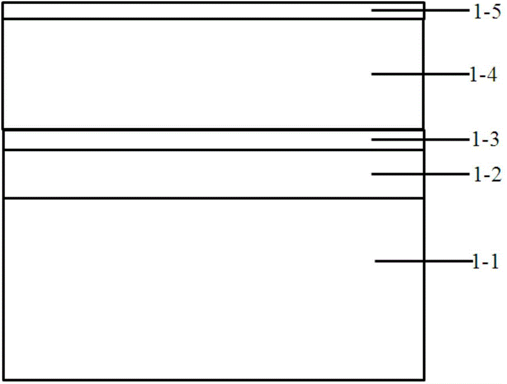
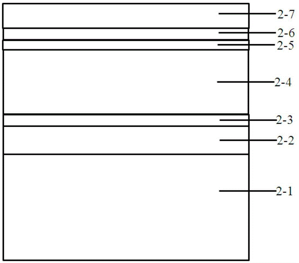
[0054] First install the 99.999% high-purity ZnO:Al target on the target position of the magnetron sputtering equipment, and then send the glass substrate 2-1 cleaned with micro-90 in step 1 into the magnetron sputtering equipment Vacuum chamber and heat to 200℃; vacuumize the vacuum chamber to less than 10 -4 Pa, fill the vacuum chamber with argon gas to 2 Pa, turn on the radio frequency power supply, adjust the power supply output power to 180W, the distance between the target and the glass substrate is 11cm, under this process sputter deposition of 1.0μm thick ZnO:Al transparent Conductive electrode layer (TCO) 2-2. Then, the glass substrate 2-1 deposited with the transparent conductive electrode layer 2-2 was put into the vacuum chamber of the magnetron sputtering device and heated to 250°C. Vacuum the vacuum chamber to less than 10 -4 Pa, fill the vacuum chamber with argon gas to 3 Pa, turn on the RF power supply, adjust the power supply output power to 40W, and the distan...
Embodiment 2
[0058] First install the 99.999% high-purity ZnO:B target material on the target position of the magnetron sputtering equipment, and then send the glass substrate 2-1 cleaned with micro-90 into the vacuum chamber of the magnetron sputtering equipment , And keep it at 25℃; evacuate the vacuum chamber to less than 10 -4 Pa, the vacuum chamber is filled with argon gas to 2Pa, the flow rate of Ar is 10sccm, the radio frequency power is turned on, the output power of the power is adjusted to 140W, the distance between the target and the glass substrate 2-1 is 11cm, and the sputtering is performed under this process A 1.0 μm thick ZnO:B transparent conductive electrode layer (TCO) 2-2 is deposited. Then, the glass substrate 2-1 on which the transparent conductive electrode layer 2-2 was deposited was put into the vacuum chamber of the magnetron sputtering device and kept at 25°C. Vacuum the vacuum chamber to less than 10 -4 Pa, the vacuum chamber is filled with argon to 3 Pa, the flo...
Embodiment 3
[0061] The surface of the mica substrate 2-1 cleaned with micro-90 is prepared by a chemical vapor deposition method to prepare a graphene transparent conductive electrode layer 2-2. The graphene growth method is as follows: prepare graphene in a tube furnace by chemical vapor deposition, put 0.5mm thick Cu foil into the tube furnace, and then heat the tube furnace to 1000°C, and pass methane and hydrogen into it. Keep it at 1000°C for 15 minutes to obtain the required graphene. Then transfer the graphene to polymethyl methacrylate (PMMA) through a solution of ferric chloride and hydrochloric acid. After placing the graphene on the mica substrate 2-1, dissolve the polymethyl methacrylate through acetone To obtain a 0.3 nm thick transparent conductive electrode layer 2-2 on the mica substrate 2-1. Then, the mica substrate 2-1 deposited with the transparent conductive electrode layer 2-2 was put into the vacuum chamber of the magnetron sputtering device and heated to 600°C. Vac...
PUM
 Abstract
Description
Claims
Application Information