P-type epitaxial layer of LED, manufacturing method thereof and LED epitaxial wafer comprising thereof

A manufacturing method and epitaxial layer technology, applied in the direction of electrical components, circuits, semiconductor devices, etc., can solve the problems of inability to effectively block electron migration, InGaN layer precipitation, and reduce luminous efficiency, so as to reduce damage, improve luminous efficiency, The effect of improving the mobility

Active Publication Date: 2014-09-24
XIANGNENG HUALEI OPTOELECTRONICS
View PDF5 Cites 18 Cited by
  • Summary
  • Abstract
  • Description
  • Claims
  • Application Information

AI Technical Summary

Problems solved by technology

[0004] In the above-mentioned LED epitaxial wafer, since the growth temperature of the P-type AlGaN electron blocking layer 61' and the high-temperature P-type GaN is much higher than the growth temperature of the InGaN layer in the quantum well layer 50', it will cause In to precipitate in the InGaN layer, resulting in quantum well damage, thereby reducing the luminous efficiency of the LED
At the same time, the P-type AlGaN electron blocking layer 61' cannot effectively block the migration of electrons in the quantum well layer 50' into the p-type epitaxial layer 60', so that the electrons migrating to the p-type epitaxial layer 60' and the holes in the p-type epitaxial layer 60' generate Non-radiative recombination, which further reduces the luminous efficiency of the LED

Method used


Image

  • P-type epitaxial layer of LED, manufacturing method thereof and LED epitaxial wafer comprising thereof
  • P-type epitaxial layer of LED, manufacturing method thereof and LED epitaxial wafer comprising thereof
  • P-type epitaxial layer of LED, manufacturing method thereof and LED epitaxial wafer comprising thereof

Examples


Embodiment approach

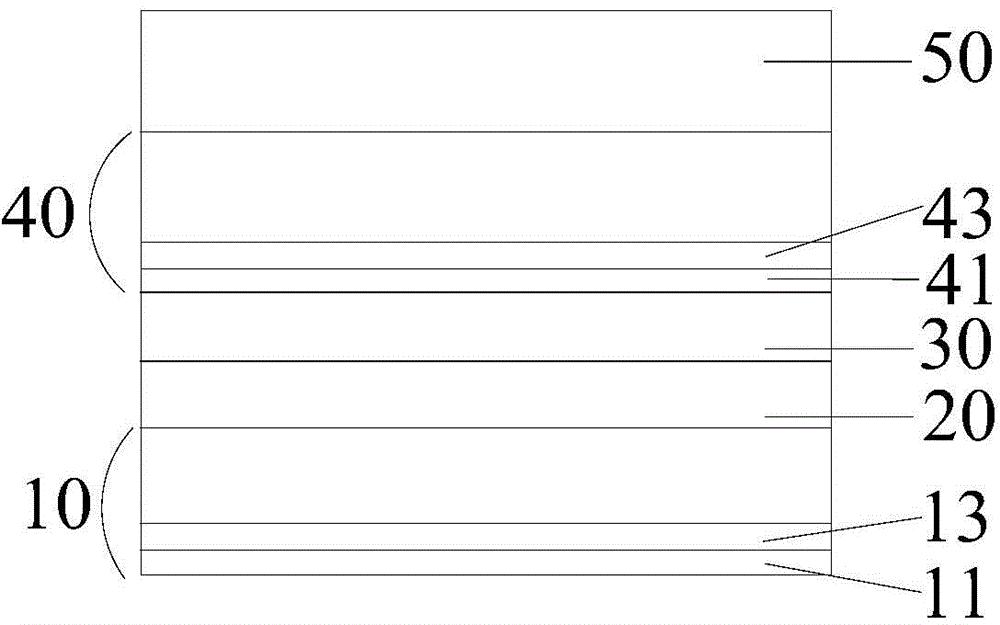
[0055] As an example, an optional implementation of forming a GaN buffer layer, u-type GaN, n-type epitaxial layer and quantum well layer is given below, including the following steps:

[0056] Place the sapphire substrate in the MOCVD reaction chamber, and use H 2 or NH 3 Wait for the gas to treat the sapphire substrate at high temperature for 5 to 10 minutes;

[0057] Lower the temperature in the reaction chamber to 500-600°C (the optimum temperature is 550°C), and feed TMGa and NH 3 , the pressure is controlled at 300torr~650torr, and a GaN buffer layer with a thickness of 15~40nm is grown on the sapphire substrate;

[0058] Raise the temperature to 950-1100°C, high-temperature annealing for 200-500s; adjust the temperature to 1000-1100°C, and feed TMGa and NH 3 , the pressure is controlled at 300torr~700torr, the first u-type GaN with a thickness of 0.8~1.2um is grown on the GaN buffer layer, and then the temperature is raised to 1050~1100℃, the pressure is controlled a...

Embodiment 1

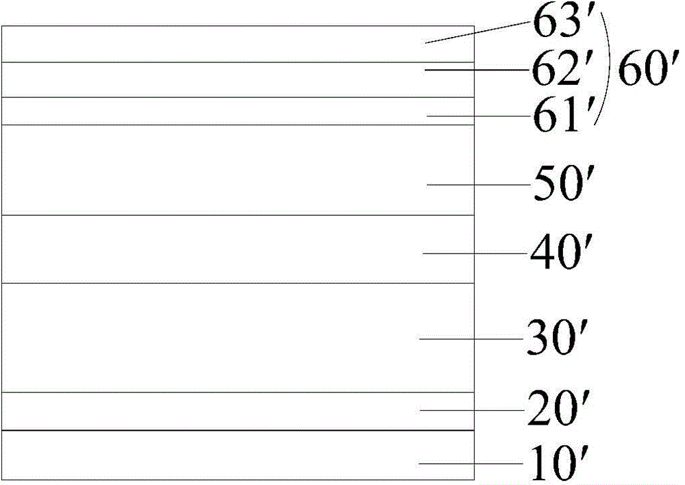
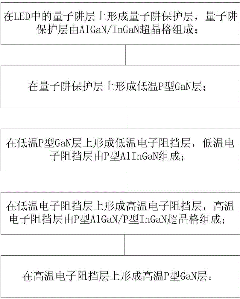
[0067] This embodiment provides a method for manufacturing an LED epitaxial wafer, including sequentially forming a GaN buffer layer, u-type GaN, n-type epitaxial layer, stress release layer, quantum well layer, and p-type epitaxial layer on a sapphire substrate along the direction away from the sapphire substrate. The step of epitaxial layer, wherein the step of forming P-type epitaxial layer comprises:

[0068] A quantum well protective layer (composed of AlGaN / InGaN superlattice) is grown on the quantum well layer (MQW), where the growth conditions are controlled at a pressure of 100torr-300torr, and the temperature is adjusted to 830°C to grow the AlGaN / InGaN superlattice layer, AlGaN The thickness of the single layer is controlled at 2nm, the thickness of the InGaN single layer is controlled at 2nm, the cycle is 5, and the total thickness is controlled at 20nm;

[0069] The temperature is adjusted to 780°C, the pressure is controlled at 100torr, and the concentration of M...


PUM


Abstract

The invention discloses a P-type epitaxial layer of an LED, a manufacturing method thereof and an LED epitaxial wafer comprising thereof. The P-type epitaxial layer comprises a quantum well protection layer which is arranged on a quantum well layer of the LED, wherein the quantum well protection layer is formed by AlGaN / InGaN superlattice; a low-temperature P-type GaN layer which is arranged on the quantum well protection layer; a low-temperature electron barrier layer which is arranged on the low-temperature P-type GaN layer and is formed by P-type AlInGaN; a high-temperature electron barrier layer which is arranged on the low-temperature electron barrier layer and is formed by P-type AlGaN / P-type InGaN superlattice; and a high-temperature P-type GaN layer which is arranged on the high-temperature electron barrier layer. The high temperature growth process of the P-type epitaxial layer causes less damage to the quantum well layer, and nonradiative recombination happening between the electrons entering the P-type epitaxial layer from the quantum well layer and holes in the P-type epitaxial layer is allowed to be reduced, thereby improving the luminous efficiency of the LED.

Description

technical field [0001] The invention relates to the technical field of semiconductor lighting, in particular to a P-type epitaxial layer of an LED, a manufacturing method thereof, and an LED epitaxial sheet comprising the same. Background technique [0002] Light-emitting diode (LED), as a new type of high-efficiency, environmentally friendly and green solid-state lighting source, has the advantages of small size, light weight, long life, high reliability and low power consumption. GaN-based semiconductor materials have good chemical and thermal stability and high breakdown voltage, and are the third-generation new semiconductor materials after the first-generation silicon materials and the second-generation gallium arsenide materials. Its bandgap is continuously adjustable from 0.7eV to 3.4eV, and its emission wavelength covers the region of visible light and near-ultraviolet light. It is the most commonly used material for the production of high-brightness blue, green and ...

Claims


Application Information

Patent Timeline
Patent Type & Authority Applications(China)
IPC IPC(8): H01L33/04H01L33/00
CPCH01L33/0075H01L33/04H01L33/145
Inventor 马欢田艳红徐迪季辉王新建
Owner XIANGNENG HUALEI OPTOELECTRONICS
Why Eureka
Try Eureka