

Organic light-emitting diode and preparation method thereof
An electroluminescence device and electroluminescence technology, which are applied in the directions of organic semiconductor devices, materials of organic semiconductor devices, and electric solid devices, etc., to achieve the effect of improving light transmittance, improving flexibility, and reducing the influence of light efficiency.
- Summary
- Abstract
- Description
- Claims
- Application Information
AI Technical Summary
Problems solved by technology
Method used
Image

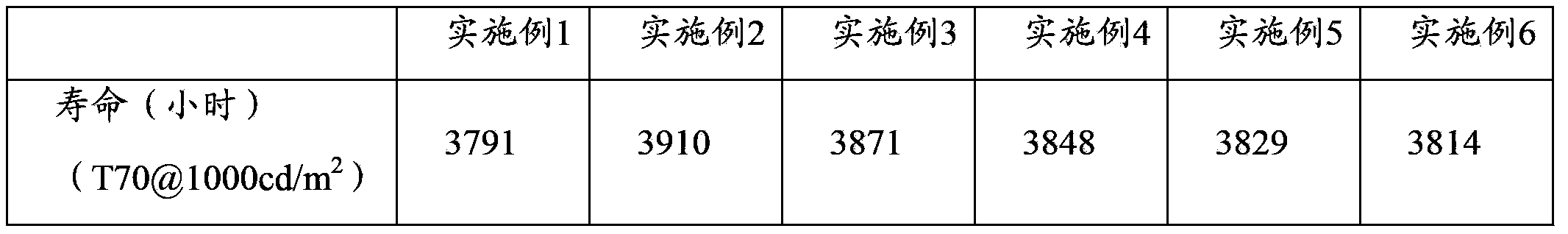
Examples
Embodiment 1
[0053] A method for preparing an organic electroluminescent device, comprising the following steps:
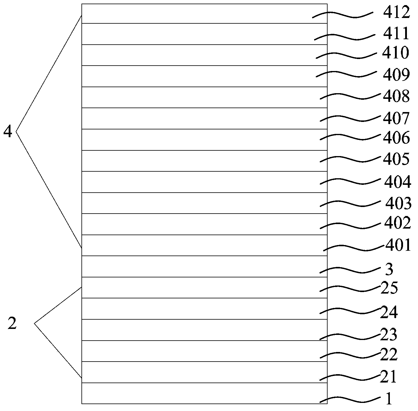
[0054] (1) Pre-treatment of ITO glass substrate 1: put ITO conductive glass substrate 1 into acetone, ethanol, deionized water, and ethanol in sequence, ultrasonically clean them for 5 minutes, then blow dry with nitrogen, and dry them in an oven for later use; The cleaned ITO glass substrate 1 is subjected to surface activation treatment to increase the oxygen content of the conductive surface layer and improve the work function of the conductive layer surface; the thickness of the ITO glass substrate 1 is 100nm;
[0055] (2) Preparation of luminescent functional layer 2:
[0056] Hole injection layer 21: MoO is evaporated on the ITO glass substrate 1 3 Hybrid material obtained by doping NPB, MoO 3 The doping mass fraction is 30%, and the evaporation is carried out by high-vacuum coating equipment, and the vacuum degree during evaporation is 1×10 -5 Pa, the evaporation rat...
Embodiment 2
[0073] A method for preparing an organic electroluminescent device, comprising the following steps:
[0074] (1), (2), (3) are the same as embodiment 1;
[0075] (4) Preparation of encapsulation layer:
[0076] (a) Preparation of the first organic barrier layer: TAPC was vacuum-evaporated on the cathode layer to obtain a first organic barrier layer with a thickness of 200 nm and a vacuum degree of 1×10 -5 Pa, the evaporation rate is
[0077] (b) Preparation of the second organic barrier layer: Bphen was vacuum evaporated on the first organic barrier layer to obtain a second organic barrier layer with a thickness of 200 nm and a vacuum degree of 1×10 -5 Pa, the evaporation rate is
[0078] (c) Preparation of the first inorganic barrier layer: a first inorganic barrier layer with a thickness of 100 nm was prepared on the second organic barrier layer by magnetron sputtering, and the material of the first inorganic barrier layer was TiO 2 , the background vacuum is 1×10 -5 ...
Embodiment 3
[0086] A method for preparing an organic electroluminescent device, comprising the following steps:
[0087] (1), (2), (3) are the same as embodiment 1;
[0088] (4) Preparation of encapsulation layer:
[0089] (a) Preparation of the first organic barrier layer: NPB was vacuum-evaporated on the cathode layer to obtain a first organic barrier layer with a thickness of 300 nm, and the vacuum degree was 1×10 -4 Pa, the evaporation rate is
[0090] (b) Preparation of the second organic barrier layer: BCP was vacuum evaporated on the first organic barrier layer to obtain a second organic barrier layer with a thickness of 300 nm, and the vacuum degree was 1×10 -4 Pa, the evaporation rate is
[0091] (c) Preparation of the first inorganic barrier layer: on the second organic barrier layer, a first inorganic barrier layer with a thickness of 50 nm was prepared by magnetron sputtering. The material of the first inorganic barrier layer was MgO, and the background vacuum degree wa...
PUM
 Abstract
Description
Claims
Application Information