White organic light-emitting diode and manufacturing method thereof

An electroluminescent device, organic technology, applied in the direction of organic semiconductor devices, electric solid devices, semiconductor/solid device manufacturing, etc., can solve the problems of high working current and low color rendering index

Inactive Publication Date: 2014-10-01
OCEANS KING LIGHTING SCI&TECH CO LTD +2
View PDF8 Cites 0 Cited by
  • Summary
  • Abstract
  • Description
  • Claims
  • Application Information

AI Technical Summary

Problems solved by technology

However, traditional white organic electroluminescent devices have the problems of low color rendering index and high operating current.

Method used


Image

  • White organic light-emitting diode and manufacturing method thereof
  • White organic light-emitting diode and manufacturing method thereof

Examples


preparation example Construction

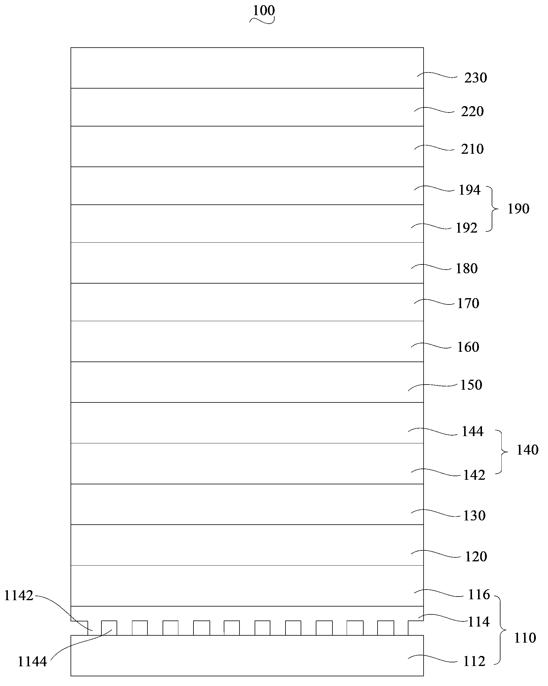
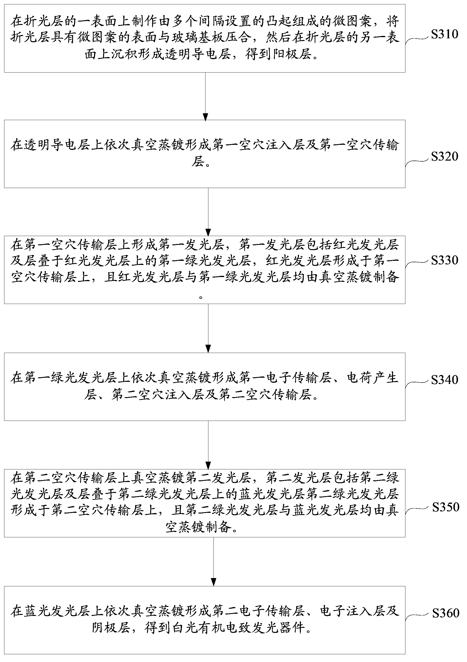
[0068] like figure 2 As shown, a method for preparing a white light organic electroluminescent device in one embodiment includes the following steps:

[0069] Step S310: On one surface of the refraction layer, a micropattern consisting of a plurality of protrusions arranged at intervals is made, and the surface of the refraction layer with the micropatterns is pressed against the glass substrate, and then deposited on the other surface of the refraction layer to form a transparent The conductive layer is used to obtain the anode layer, wherein a plurality of gaps are formed between the refraction layer and the glass substrate.

[0070] Preferably, before pressing the surface of the refraction layer with the micropattern on the glass substrate, it also includes the steps of sequentially cleaning and surface activating the glass substrate; the cleaning step is: sequentially wash the glass substrate with detergent, deionized water, Ultrasonic cleaning with acetone and ethanol, ...

Embodiment 1

[0093]The structure of the white light organic electroluminescence device of the present embodiment is: ITO / PU / ITO / NPB:MoO 3 / NPB / TCTA:Ir(MDQ) 2 (acac) / TCTA:Ir(ppy) 3 / Bphen / MoO 3 / NPB:MoO 3 / NPB / TCTA:Ir(ppy) 3 / CBP:Firpic:MoO 3 / Bphen / Bphen:Cs 2 CO 3 / Ag.

[0094] The preparation of the white light organic electroluminescent device of this embodiment is as follows:

[0095] (1) Clean the ITO glass substrate with a thickness of 100 nanometers sequentially with detergent, deionized water, acetone and ethanol ultrasonically, wash for 5 minutes each time, stop for 5 minutes, repeat 3 times respectively, and then dry it in an oven. After drying, the glass substrate is subjected to surface activation treatment; on one surface of the refraction layer, a micro-pattern consisting of a plurality of protrusions arranged at intervals is made. The width of each protrusion is 5 microns, and the height is 5 microns. The distance between the two protrusions is 5 microns; the surface...

Embodiment 2

[0102] The structure of the white light organic electroluminescence device of the present embodiment is: ITO / PU / AZO / TCTA:WO 3 / TCTA / mCP:PQIr / mCP:Ir(ppy) 2 (acac) / BCP / V 2 o 5 / TCTA:WO 3 / TCTA / mCP:Ir(ppy) 2 (acac) / mCP:FIr6:V 2 o 5 / BCP / BCP:CsF / Al.

[0103] The preparation of the white light organic electroluminescent device of this embodiment is as follows:

[0104](1) Clean the ITO glass substrate with a thickness of 100 nanometers sequentially with detergent, deionized water, acetone and ethanol ultrasonically, wash for 5 minutes each time, stop for 5 minutes, repeat 3 times respectively, and then dry it in an oven. After drying, the glass substrate is subjected to surface activation treatment; on one surface of the refraction layer, a micro-pattern consisting of a plurality of protrusions arranged at intervals is made, each protrusion has a width of 10 microns and a height of 10 microns, and two adjacent The distance between the two protrusions is 10 microns; the surf...


PUM

PropertyMeasurementUnit
Thicknessaaaaaaaaaa
Lumen efficiencyaaaaaaaaaa

Abstract

A white organic light-emitting diode comprises an anode layer, a first hole injection layer, a first hole transmission layer, a first light-emitting layer, a first electron transmission layer, a charge generation layer, a second hole injection layer, a second hole transmission layer, a second light-emitting layer, a second electron transmission layer, an electron injection layer and a cathode layer, wherein the anode layer, the first hole injection layer, the first hole transmission layer, the first light-emitting layer, the first electron transmission layer, the charge generation layer, the second hole injection layer, the second hole transmission layer, the second light-emitting layer, the second electron transmission layer, the electron injection layer and the cathode layer are stacked in sequence. The anode layer comprises a glass substrate, a refraction layer and a transparent conducting layer, wherein the glass substrate, the refraction layer and the transparent conducting layer are stacked in sequence. The surface, opposite to the glass substrate, of the refraction layer is provided with a micro-pattern composed of a plurality of protrusions arranged at intervals, and therefore a plurality of gaps are formed between the refraction layer and the glass substrate. The first light-emitting layer comprises a red light-emitting layer body and a first green light-emitting layer body stacked on the red light-emitting layer body. The second light-emitting layer comprises a second green light-emitting layer body and a blue light-emitting layer body stacked on the second green light-emitting layer body. The white organic light-emitting diode has a higher color rendering index and a lower working current. The invention further relates to a manufacturing method of the white organic light-emitting diode.

Description

technical field [0001] The invention relates to the field of electronic devices, in particular to a white light organic electroluminescent device and a preparation method thereof. Background technique [0002] White light organic electroluminescent devices (OLEDs) have some unique advantages: (1) OLEDs are diffuse surface light sources, and do not require an additional light guide system to obtain large-area white light sources like light-emitting diodes (LEDs); (2) ) Due to the diversity of organic light-emitting materials, OLED lighting can design the required color of light according to needs. At present, both small molecule OLEDs and polymer organic light-emitting diodes (PLEDs) have obtained all colors including white light spectrum. (3) OLED can be made on a variety of substrates such as glass, ceramics, metal, plastic and other materials, which makes the design of lighting sources more free; (4) OLED lighting panels can be made in the way of making OLED displays Disp...

Claims


Application Information

Patent Timeline
IPC IPC(8): H01L51/52H01L51/54H01L51/56C23C14/04
CPCH10K85/615H10K85/342H10K85/6572H10K50/131H10K50/858H10K2102/00H10K71/00
Inventor 周明杰钟铁涛王平陈吉星
Owner OCEANS KING LIGHTING SCI&TECH CO LTD
Why Eureka
Try Eureka