

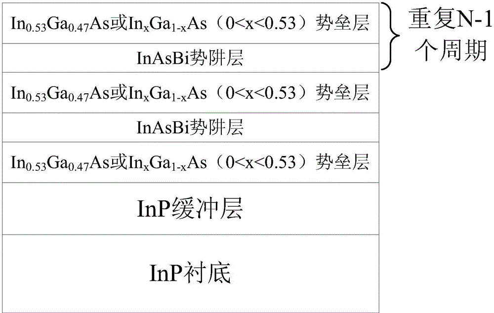
InP-based intermediate infrared InAsBi quantum well structure
A quantum well and infrared technology, applied in phonon exciters, laser parts, electrical components, etc., can solve the problem that the light emission wavelength is difficult to break through 3 microns, and achieve high electro-optical conversion efficiency, excellent substrate quality, and threshold current low effect
- Summary
- Abstract
- Description
- Claims
- Application Information
AI Technical Summary
Problems solved by technology
Method used
Image

Examples
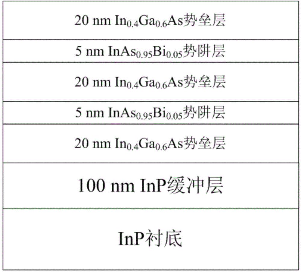
Embodiment 1
[0019] To prepare InAs with an InP-based emission wavelength of 3.1 microns 0.95 Bi 0.05 Double quantum well as an example:
[0020] (1) To grow InAs on an InP substrate 0.95 Bi 0.05 Double quantum well structure, first grow a 100nm InP buffer layer;
[0021] (2) grow a layer of 20nm thick In 0.4 Ga 0.6 As material as a barrier layer;
[0022] (3) Grow a layer of InAs with a thickness of 5nm 0.95 Bi 0.05 material as a potential well layer;
[0023] (4) Grow a layer of In with a thickness of 20nm again 0.4 Ga 0.6 As material as a barrier layer;
[0024] (5) A layer of InAs with a thickness of 5nm is grown again 0.95 Bi 0.05 material as a potential well layer for the second quantum well;
[0025] (6) Finally grow a layer of In with a thickness of 20nm 0.4 Ga 0.6 The As material is used as a barrier layer to complete the growth of the double quantum well structure, and the quantum well emits light at room temperature with a wavelength of about 3.1 microns.
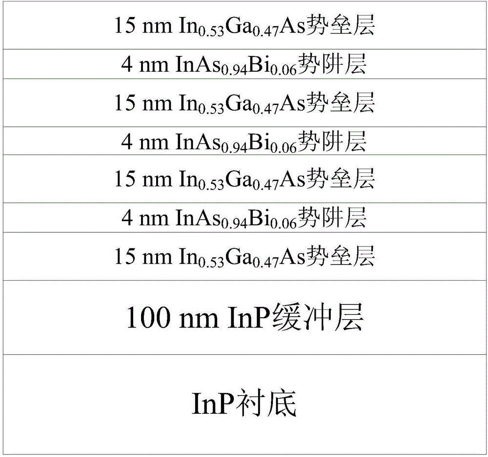
Embodiment 2
[0027] To prepare InAs with an InP-based emission wavelength of 3.0 microns 0.94 Bi 0.06 Three quantum wells as an example:
[0028] (1) To grow InAs on an InP substrate 0.94 Bi 0.06 Three quantum well structure, first grow a 100nm InP buffer layer;
[0029] (2) grow a layer of 15nm thick In 0.53 Ga 0.47 As material as a barrier layer;
[0030] (3) grow a layer of 4nm thick InAs 0.94 Bi 0.06 material as a potential well layer;
[0031] (4) grow a layer of 15nm thick In again 0.53 Ga 0.47 As material as a barrier layer;
[0032] (5) The above-mentioned (3) and (4) processes are repeated twice in a cycle, that is, the growth of the three-quantum well structure is completed, and the emission wavelength of the quantum wells at room temperature is about 3.0 microns.
PUM
 Abstract
Description
Claims
Application Information