Semi-polar planar GaN-based light emitting diode and preparation method

A light-emitting diode and semi-polar surface technology, which is applied in semiconductor devices, electrical components, circuits, etc., can solve the problems of limited space for improvement and low light extraction efficiency of semi-polar surface LEDs, so as to improve crystal quality and improve current expansion , the effect of suppressing dislocation generation

Inactive Publication Date: 2014-10-22
INST OF SEMICONDUCTORS - CHINESE ACAD OF SCI
View PDF7 Cites 19 Cited by
  • Summary
  • Abstract
  • Description
  • Claims
  • Application Information

AI Technical Summary

Problems solved by technology

The high-density dislocations and stacking faults in the semipolar GaN epitaxial layer originate from the film-substrate interface. In epitaxy, the method of adjusting the growth mode through substrate nitridation combined with buffer layer opti

Method used


Image

  • Semi-polar planar GaN-based light emitting diode and preparation method
  • Semi-polar planar GaN-based light emitting diode and preparation method
  • Semi-polar planar GaN-based light emitting diode and preparation method

Examples


Embodiment Construction

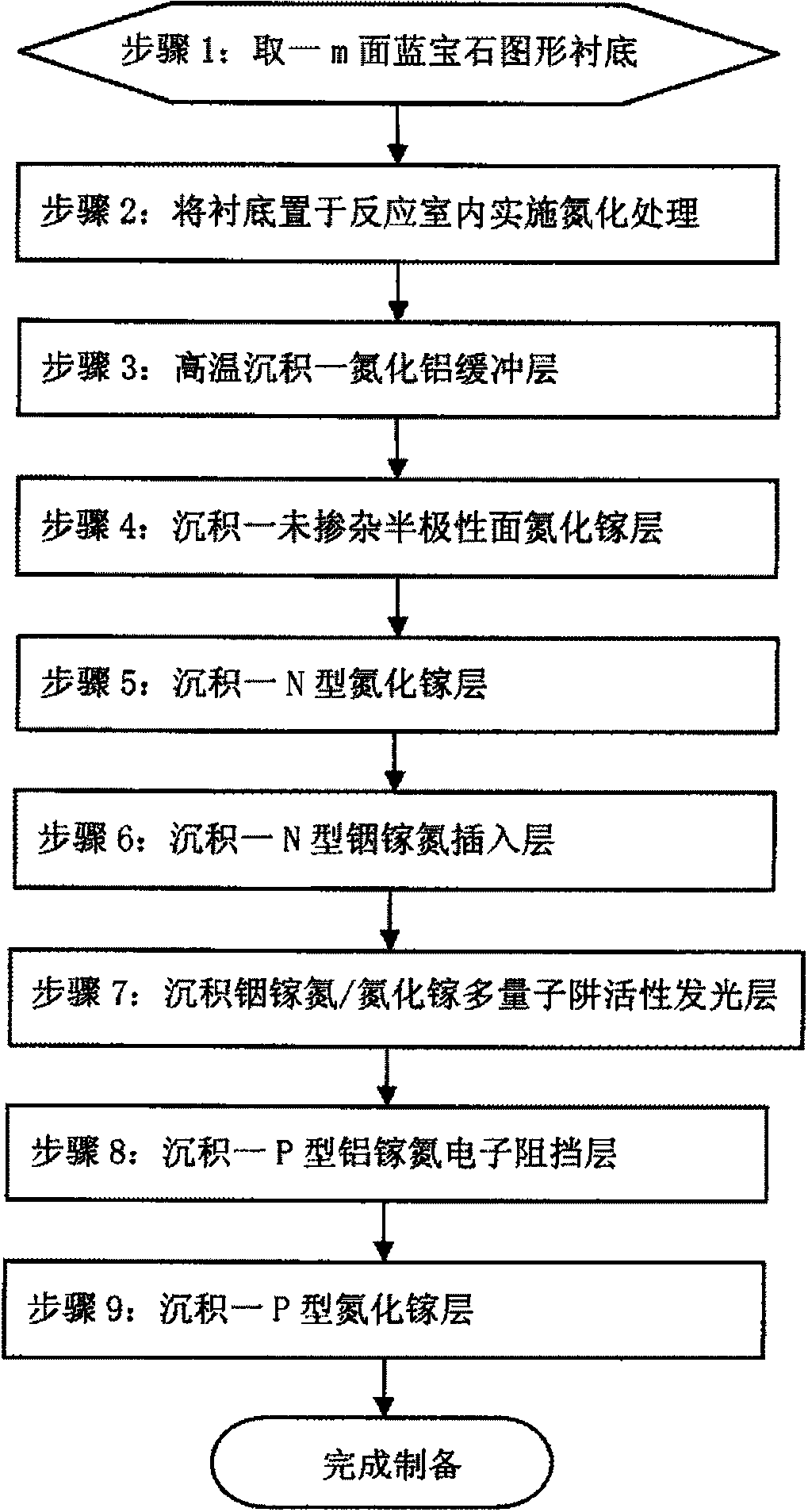
[0038]The invention prepares a semipolar (11-22) surface gallium nitride-based light-emitting diode with a special orientation. On the one hand, it effectively suppresses the internal quantum efficiency attenuation caused by the quantum-confined Stark effect in traditional devices, and on the other hand, it improves the quantum well indium The incorporation rate of the components can extend the emission wavelength of GaN-based light-emitting diodes to the dark green or even orange light region.

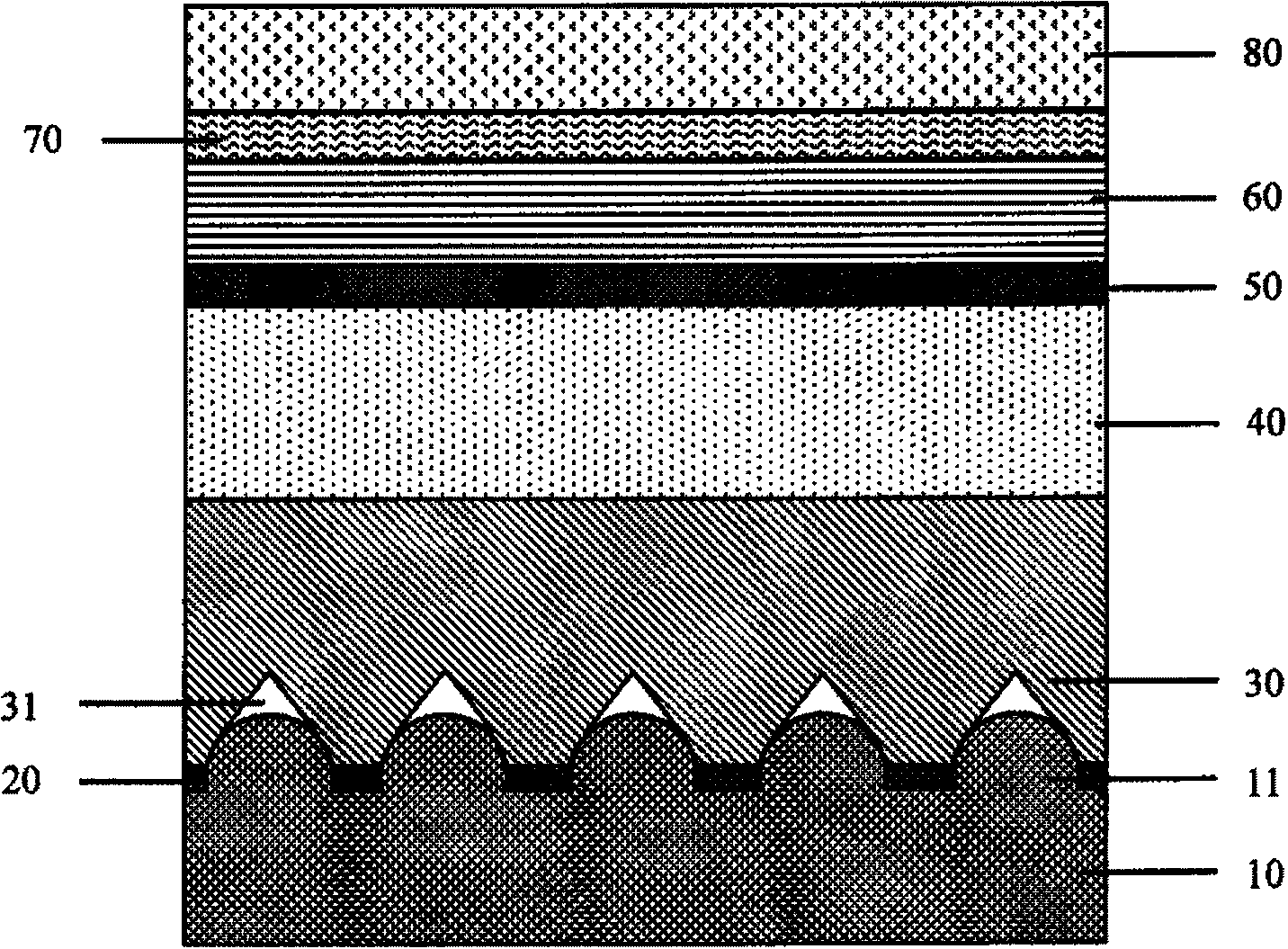
[0039] see figure 1 As shown, the present invention provides a semi-polar gallium nitride-based light-emitting diode, including:

[0040] A substrate 10, the surface of which has raised patterns 11 arranged periodically. The substrate 10 is a sapphire substrate with an orientation (10-10) m plane, and the period of the raised patterns 11 on its surface is 3-7 μm, and the diameter of the bottom is It is 2-4 μm, the height is 1-2 μm, and the interval between each raised pattern 11 is 1...


PUM

PropertyMeasurementUnit
Bottom diameteraaaaaaaaaa
Heightaaaaaaaaaa
Thicknessaaaaaaaaaa

Abstract

The invention provides a semi-polar planar GaN-based light emitting diode and its preparation method. The light emitting diode comprises a substrate, an aluminium nitride buffer layer, an undoped semi-polar planar GaN layer, a semi-polar planar GaN N-type layer, a semi-polar planar N-type InGaN insert layer, a semi-polar planar GaN/InGaN multiple quantum well active luminescent layer, a semi-polar planar P-type AlGaN electronic barrier layer, and a semi-polar planar P-type GaN layer. The surface of the substrate has raised graphs which are periodically arranged; the aluminium nitride buffer layer is deposited in interval areas among the raised graphs; the undoped semi-polar planar GaN layer is manufactured on the aluminium nitride buffer layer; there are gas areas between the undoped semi-polar planar GaN layer and the raised graphs on the surface of the substrate, thus blocking dislocation defects from extending upwards; the semi-polar planar GaN N-type layer is manufactured on the undoped semi-polar planar GaN layer; the semi-polar planar N-type InGaN insert layer is manufactured on the semi-polar planar GaN N-type layer; the semi-polar planar GaN/InGaN multiple quantum well active luminescent layer is manufactured on the semi-polar planar N-type InGaN insert layer; the semi-polar planar P-type AlGaN electronic barrier layer is manufactured on the semi-polar planar GaN/InGaN multiple quantum well active luminescent layer; and the semi-polar planar P-type GaN layer is manufactured on the semi-polar planar P-type AlGaN electronic barrier layer.

Description

technical field [0001] The invention belongs to the technical field of semiconductors and relates to light-emitting diodes, in particular to a semi-polar (11-22) surface gallium nitride-based light-emitting diode (LED) structure based on an m-plane sapphire pattern substrate and a preparation method thereof. The combination of pattern substrate growth technology and indium gallium nitrogen insertion layer technology can significantly improve the crystal quality and surface morphology of light-emitting diode materials, and improve the light extraction efficiency of semi-polar surface gallium nitride-based light-emitting diodes. Background technique [0002] As a typical application of the third-generation wide-bandgap semiconductor technology, commercial gallium nitride (GaN)-based LED products have covered the ultraviolet to green light spectrum. As a light-emitting device, GaN-based LEDs can be widely used in many aspects such as indoor and outdoor lighting, commercial ligh...

Claims


Application Information

Patent Timeline
IPC IPC(8): H01L33/16H01L33/18H01L33/32H01L33/20H01L33/06H01L33/12H01L33/00
CPCH01L33/0066H01L33/0075H01L33/06H01L33/12H01L33/18H01L33/22H01L33/325
Inventor 项若飞汪连山赵桂娟金东东王建霞李辉杰张恒冯玉霞焦春美魏鸿源杨少延王占国
Owner INST OF SEMICONDUCTORS - CHINESE ACAD OF SCI
Why Eureka
Try Eureka