

Multi-layer flexible plane embedded laminated electrode, preparation method of electrode, and application of electrode in organic single crystal field effect transistor
A planar and laminated technology, applied in the field of organic electronics, can solve the problems of forming air gaps, organic semiconductors that cannot be bonded with insulating layers, and affecting device performance, and achieve high integration, reuse, and high precision.
- Summary
- Abstract
- Description
- Claims
- Application Information
AI Technical Summary
Problems solved by technology
Method used
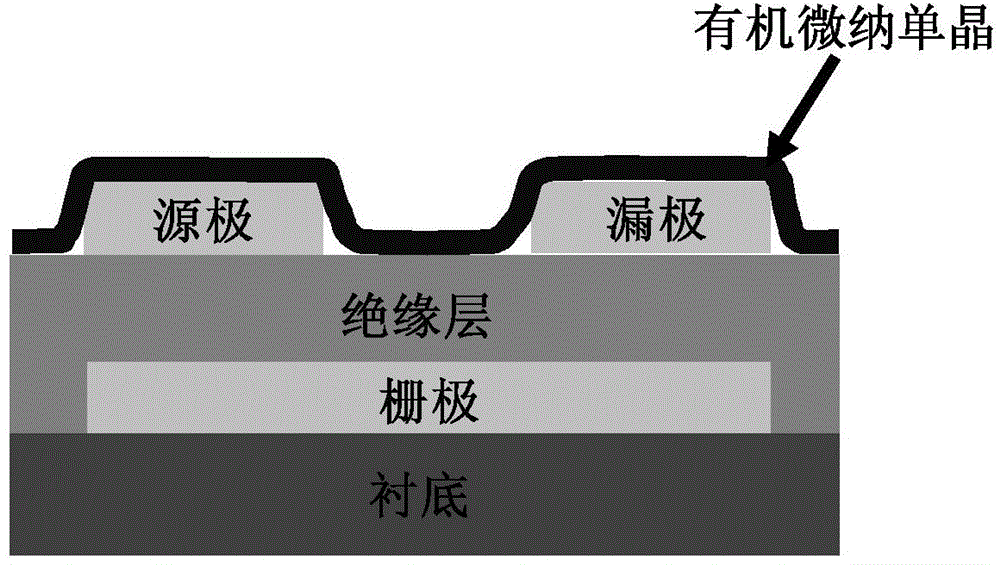
Image

Examples
Embodiment 1
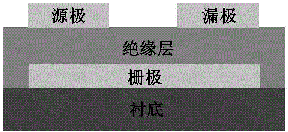
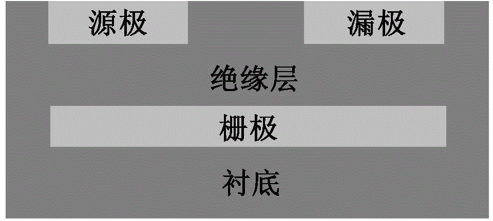
[0041] Example 1. Preparation of flexible planar embedded laminated electrodes
[0042] 1. Octadecyltrichlorosilane OTS modified silicon surface: firstly clean the substrate surface; Hydroxylation is formed on the surface of the substrate; the substrate is cleaned again; the substrate is put into the OTS solution of n-heptane with a volume ratio of 1000:1 to form a layer of OTS on the surface of the substrate.
[0043] 2. Prepare source / drain electrodes and gate electrodes by photolithography on the OTS modified substrate and modify mercaptopropyltrimethoxysilane (MPT) on the metal surface: first use AZ5214E photoresist on the substrate respectively Photolithography (baking temperature: 100 degrees; baking time: 3min; exposure time: 20s; developing time: 60s; fixing time: 30s) source / drain electrodes and gate electrodes; then vacuum evaporate a layer of gold (vacuum degree: 10 -6 torr; Evaporation rate: 0.01nm / s; Evaporation thickness: 25nm); Before removing glue, utilize ...
Embodiment 2
[0057] Example 2. Preparation of flexible planar embedded laminated electrodes
[0058] 1. Octadecyltrichlorosilane OTS modified glass surface: first clean the surface of the substrate; Hydroxylation is formed on the surface of the substrate; the substrate is cleaned again; the substrate is put into the OTS solution of n-heptane with a volume ratio of 1000:1 to form a layer of OTS on the surface of the substrate.
[0059] 2. Prepare source / drain electrodes and gate electrodes by photolithography on the OTS modified substrate and modify mercaptopropyltrimethoxysilane (MPT) on the metal surface: first use AZ5214E photoresist on the substrate respectively Photolithography (baking temperature: 100 degrees; baking time: 3min; exposure time: 20s; developing time: 60s; fixing time: 30s) source / drain electrodes and gate electrodes; then vacuum evaporate a layer of gold (vacuum degree: 10 -6 torr; Evaporation rate: 0.01nm / s; Evaporation thickness: 25nm); Before degumming, utilize v...
Embodiment 3
[0067] Example 3, preparation of flexible planar embedded laminated electrodes
[0068] 1. Octadecyltrichlorosilane OTS modified glass surface: first clean the surface of the substrate; Hydroxylation is formed on the surface of the substrate; the substrate is cleaned again; the substrate is put into the OTS solution of n-heptane with a volume ratio of 1000:1 to form a layer of OTS on the surface of the substrate.
[0069] 2. Prepare source / drain electrodes and gate electrodes by photolithography on the OTS modified substrate and modify mercaptopropyltrimethoxysilane (MPT) on the metal surface: first use AZ5214E photoresist on the substrate respectively Photolithography (baking temperature: 100 degrees; baking time: 3min; exposure time: 20s; developing time: 60s; fixing time: 30s) source / drain electrodes and gate electrodes; then vacuum evaporate a layer of gold (vacuum degree: 10 -6 torr; Evaporation rate: 0.01nm / s; Evaporation thickness: 25nm); Before degluing, utilize va...
PUM
| Property | Measurement | Unit |
|---|---|---|
| thickness | aaaaa | aaaaa |
| thickness | aaaaa | aaaaa |
| width | aaaaa | aaaaa |
Abstract
Description
Claims
Application Information