Doping method

A doped layer and impurity technology, applied in the field of doping, can solve the problems of poor process applicability, deteriorated solar cell performance, too high requirements for silicon wafer quality and purity, and achieves reduction of doping concentration, reduction of defect density, improvement of performance effect

Inactive Publication Date: 2014-11-12
KINGSTONE SEMICONDUCTOR LIMITED COMPANY
View PDF4 Cites 5 Cited by
  • Summary
  • Abstract
  • Description
  • Claims
  • Application Information

AI Technical Summary

Problems solved by technology

[0004] 1) The implanted damaged layer cannot be well repaired, especially when the lower implant dose cannot form a completely amorphized damaged layer, thereby deteriorating the performance of the solar cell thus obtained
[0005] 2) There is no additional gettering function, which leads to too high requirements on the quality and purity of silicon wafers, and the applicability of the process is not wide
Therefore, harmful impurities tend to concentrate in these two regions. Since there is no possibility of subsequent removal of the gettering layer, the performance of solar cells will be further deteriorated in the case of poor quality silicon wafers or pollution introduced by the doping process.

Method used


Image

  • Doping method
  • Doping method
  • Doping method

Examples


Embodiment 1

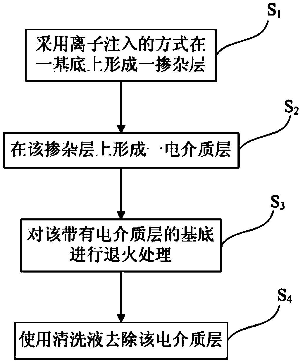
[0045] refer to figure 1 , the doping method described in this embodiment, comprising the following steps:

[0046] Step S 1 . Forming a doped layer on a substrate by means of ion implantation;

[0047] Step S 2 1. Forming a dielectric layer on the doped layer, wherein silicon nitride is formed by PECVD using silane and ammonia as the dielectric layer, and the thickness of the silicon nitride is 40nm;

[0048] Step S 3 1. Perform annealing treatment on the substrate with the dielectric layer, the annealing temperature is 850° C., and the annealing time is 60 minutes;

[0049] Step S 4 , using hydrofluoric acid as a cleaning solution to remove the dielectric layer.

[0050] The silicon nitride can uniformly reduce the doping concentration on the surface of the substrate, and the use of this doping method to manufacture solar cells will help reduce the recombination between the surface of the solar cell and the junction region. In addition, the silicon nitride also contri...

Embodiment 2

[0052] The principle of embodiment 2 is the same as embodiment 1, the only difference is:

[0053] After ion implantation, step S 2A cleaning step is also included before, to remove impurities formed by doping ions and / or metal impurities on the surface, back or sides of the substrate.

[0054] Refer to Example 1 for all the other unmentioned parts.

Embodiment 3

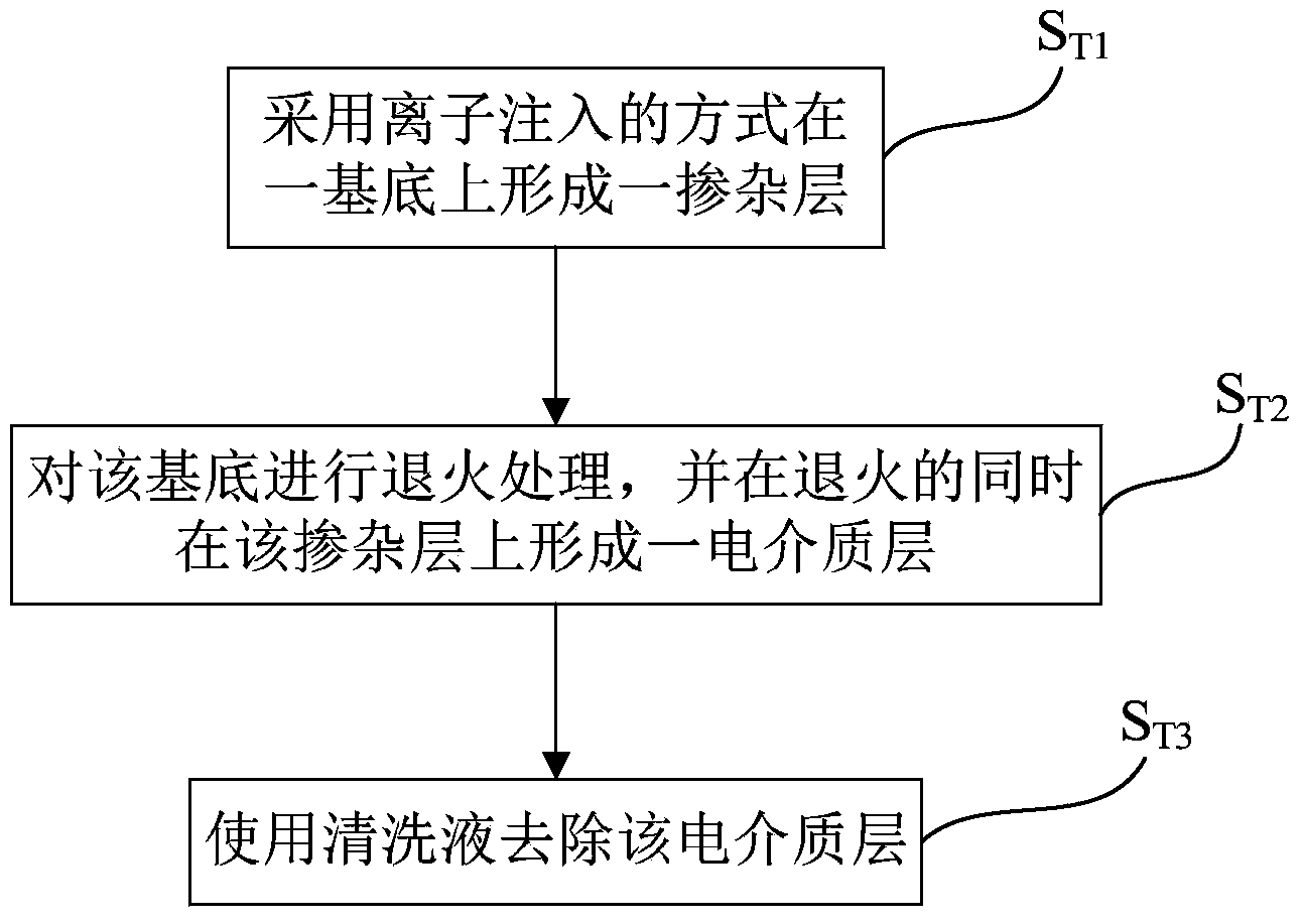
[0056] refer to figure 2 , the basic principle of embodiment 3 is the same as that of embodiment 1, the only difference is:

[0057] Step S T1 . Forming a doped layer on a substrate by means of ion implantation;

[0058] Step S T2 1. Perform annealing treatment on the substrate, and form a dielectric layer on the doped layer while annealing, wherein ammonia gas and oxygen gas are passed through during the annealing process to form silicon oxynitride as the dielectric layer;

[0059] Step S T3 , using a cleaning solution to remove the dielectric layer.


PUM

PropertyMeasurementUnit
thicknessaaaaaaaaaa
thicknessaaaaaaaaaa

Abstract

The invention discloses a doping method. The doping method includes the steps a doping layer is formed on a substrate in an ion injection mode; a dielectric layer is formed on the doping layer; annealing processing is carried out on the substrate with the dielectric layer; the dielectric layer is removed through cleaning fluids. After the doping layer is formed through ion injection, the dielectric layer is formed, and accordingly the performance of a PN structure can be improved, the dielectric layer can reduce doping concentration of the surface of the substrate and facilitate repair of lattice defects, the defect density in an injection damage layer can be obviously reduced, impurities on the substrate can be absorbed to a certain extent and accordingly influences of the harmful impurities are reduced.

Description

technical field [0001] The invention relates to a doping method, in particular to a doping method using ion implantation. Background technique [0002] In the current doping process, especially the doping method for making solar cells comprises the following steps: Step S 1 , forming a doped layer on a substrate by means of ion implantation; step S 2 , cleaning the substrate; step S 3 , annealing the substrate. [0003] The disadvantages of this method are: [0004] 1) The implanted damaged layer cannot be well repaired, especially when the lower implanted dose cannot form a completely amorphized damaged layer, thereby deteriorating the performance of the solar cell thus produced. [0005] 2) There is no additional gettering function, which leads to too high requirements on the quality and purity of silicon wafers, and the applicability of the process is not wide. [0006] 3) Implanting the damaged layer In the process of annealing to repair the damage, the implanted la...

Claims


Application Information

Patent Timeline
Patent Type & Authority Applications(China)
IPC IPC(8): H01L21/265H01L21/3105H01L21/31
CPCH01L21/265H01L21/02057H01L31/1864
Inventor 金光耀王懿喆洪俊华沈培俊
Owner KINGSTONE SEMICONDUCTOR LIMITED COMPANY
Why Eureka
Try Eureka